Active matrix type liquid crystal display device

Inactive Publication Date: 2007-08-23
WINTEK CORP
View PDF27 Cites 0 Cited by
  • Summary
  • Abstract
  • Description
  • Claims
  • Application Information

AI Technical Summary

Benefits of technology

[0011]Through the design of the invention, since the two capacitor electrodes of a storage capacitor are separated from each other only by the passivation layer, a smaller area of the capacitor electrode can be selected to maintain sufficient storage capacitance. Thus, the spread areas of opaque metallic films are decreased to result in a high aperture ratio. On the other hand, the extra areas of the lower capacitor electrode, which may be provided for maintaining a proper positioning to

Problems solved by technology

This may result in a significant decrease of the aperture ratio for the display device because the capacitor electrode is made of opaque metal

Method used


Image

  • Active matrix type liquid crystal display device
  • Active matrix type liquid crystal display device
  • Active matrix type liquid crystal display device

Examples


Embodiment Construction

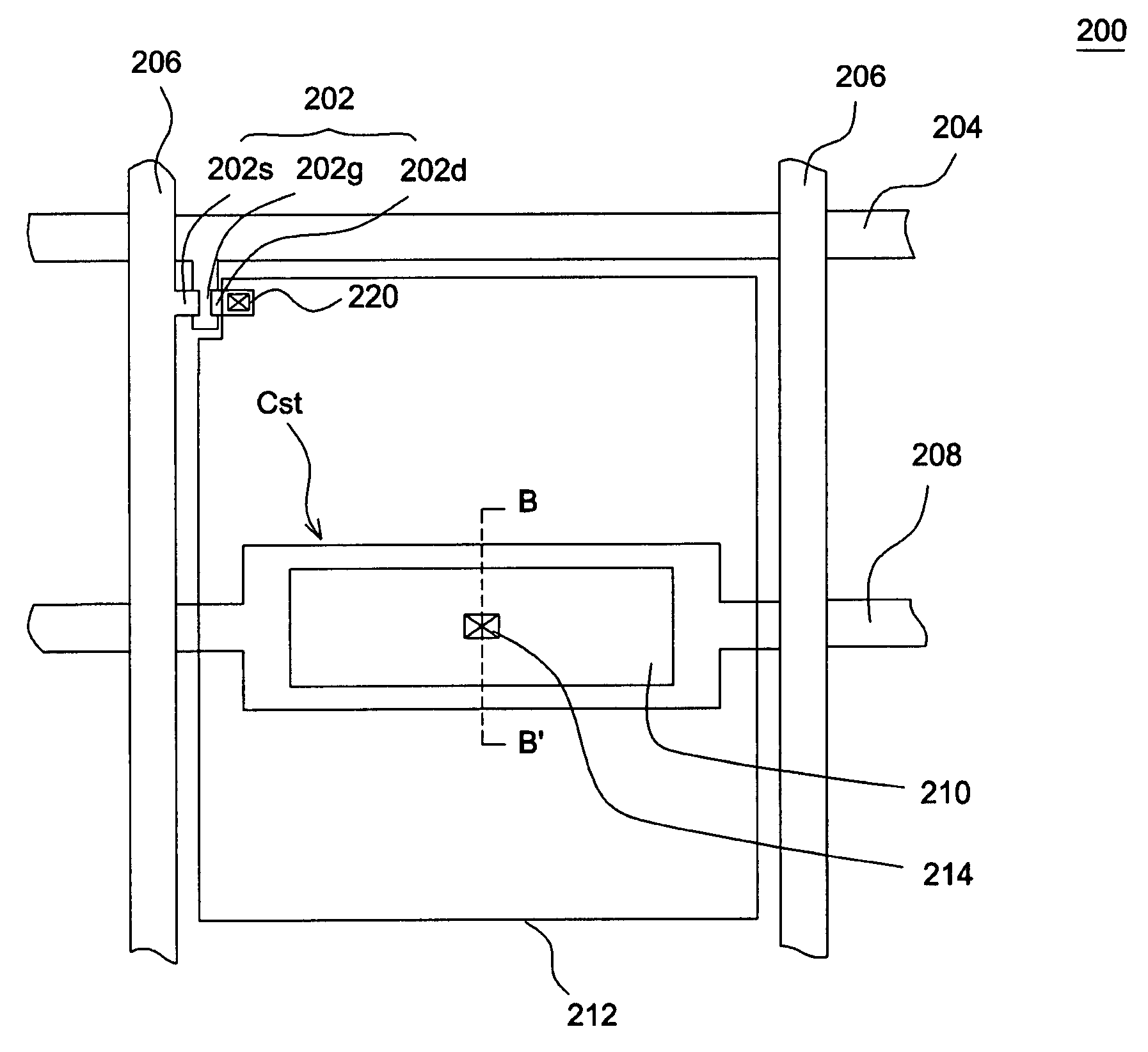
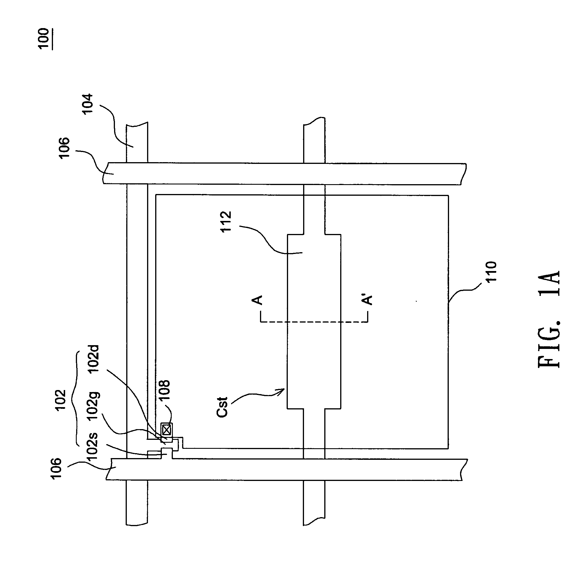
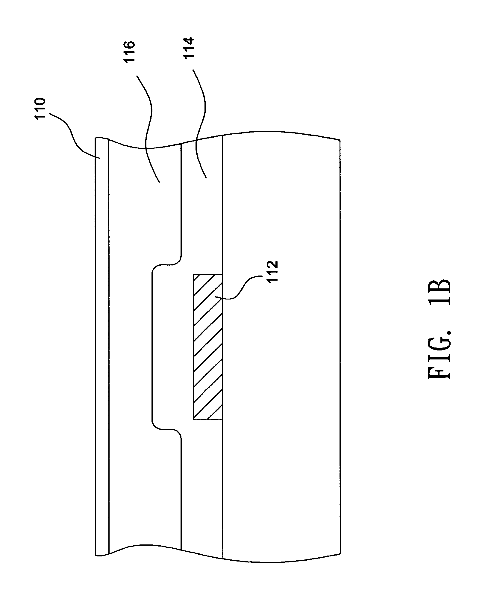
[0018]FIG. 3 shows a partial cross-sectional view illustrating an active matrix type liquid crystal display (AM LCD) device 10 according to the invention. Referring to FIG. 3, the display device 10 includes a color filter substrate 12 and an array substrate 14, with a liquid crystal layer 16 interposed between them. In the array substrate 14, a switching device such as a thin film transistor (TFT) 18, a pixel electrode 22, and a first alignment layer 24 are formed on a transparent substrate 15. Further, in the color filter substrate 12, a color filter 26, a black matrix layer 28, a common electrode 32, and a second alignment layer 34 are formed on a transparent substrate 13.

[0019]FIGS. 4A and 4B show schematic diagrams illustrating an embodiment of a pixel structure 40 of an active matrix display device according to the invention, where FIG. 4A shows a plan view observed from the normal direction of an array substrate, and FIG. 4B shows a cross-sectional view taken along line C-C′ i...


PUM


Abstract

An active matrix type liquid crystal display includes a first substrate, a second substrate, and a liquid crystal layer interposed between them. A plurality of common lines are provided on the second substrate, and a first dielectric layer provided with contact holes is fonned on the second substrate and covers the common lines. Capacitor electrodes connected to the common lines via the contact holes are provided on the first dielectric layer, and a second dielectric layer is formed overlying the capacitor electrodes. Pixel electrodes are formed on the second dielectric layer, and each pixel electrode together with each capacitor electrode form a storage capacitor.

Description

CROSS REFERENCE TO RELATED PATENT APPLICATION[0001]The present application claims priority under 35 U.S.C. §119(a) on Patent Application No. 095104149 filed in Taiwan on Feb. 8, 2006, the entire contents of which are hereby incorporated by reference.BACKGROUND OF THE INVENTION[0002](a) Field of the Invention[0003]The invention relates to an active matrix type liquid crystal display (AM LCD) device having a high aperture ratio.[0004](b) Description of the Related Art[0005]At present, the dominant method for fabricating an active matrix liquid crystal display device is typically based on amorphous silicon thin film transistor (a-Si TFT) technologies.[0006]FIG. 1A shows a plan view illustrating a conventional active matrix display device 100. FIG. 1B shows a cross-sectional view of the active matrix display device shown in FIG. 1A, taken along line A-A′. Referring to FIG. 1A, the gate 102g of an n-type a-Si TFT 102 is connected to a gate line 106, its source 102s is connected to a data...

Claims


Application Information

Patent Timeline
IPC IPC(8): H01L21/8242
CPCH01L27/1255G02F1/136213
Inventor KUO, CHIEN-CHUNGCHOU, YI-LIN
Owner WINTEK CORP
Why Eureka
Try Eureka