Pixel structure and fabrication method of pixel structure

a technology of pixel structure and fabrication method, which is applied in the direction of optics, transistors, instruments, etc., can solve the problems of inability to characterize the existing pixel structure, further limit the display aperture ratio, etc., and achieve the effect of increasing the display aperture ratio and sufficient storage capacitan

Active Publication Date: 2013-11-12
AU OPTRONICS CORP
View PDF7 Cites 0 Cited by
  • Summary
  • Abstract
  • Description
  • Claims
  • Application Information

AI Technical Summary

Benefits of technology

[0007]The invention is directed to a pixel structure having two metal layers, so as to provide sufficient storage capacitance and increase a display aperture ratio.
[0008]The invention is further directed to a fabrication method of a pixel structure with use of five photomasks, so as to form the pixel structure with high storage capacitance and high display aperture ratio.
[0020]Based on the above, in the pixel structure described in the embodiments of the invention, the capacitor electrode is disposed between the data line and the pixel electrode, such that the area occupied by the pixel electrode is expanded, and that the high display aperture ratio can be ensured. Moreover, fabrication of the pixel structure can be completed with mere use of five photomasks; therefore, the pixel structure described in the embodiments of the invention can be easily formed.

Problems solved by technology

Therefore, the pixel electrodes and the data lines must have a certain distance therebetween, which further limits the display aperture ratio.
As a result, the existing pixel structures are not apt to be characterized by both the high image quality and the ideal display aperture ratio.

Method used


Image

  • Pixel structure and fabrication method of pixel structure
  • Pixel structure and fabrication method of pixel structure
  • Pixel structure and fabrication method of pixel structure

Examples


Embodiment Construction

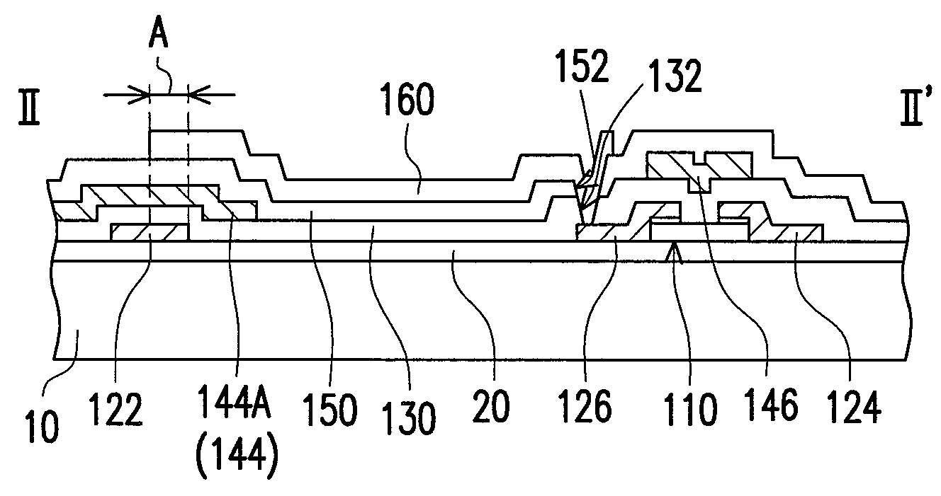
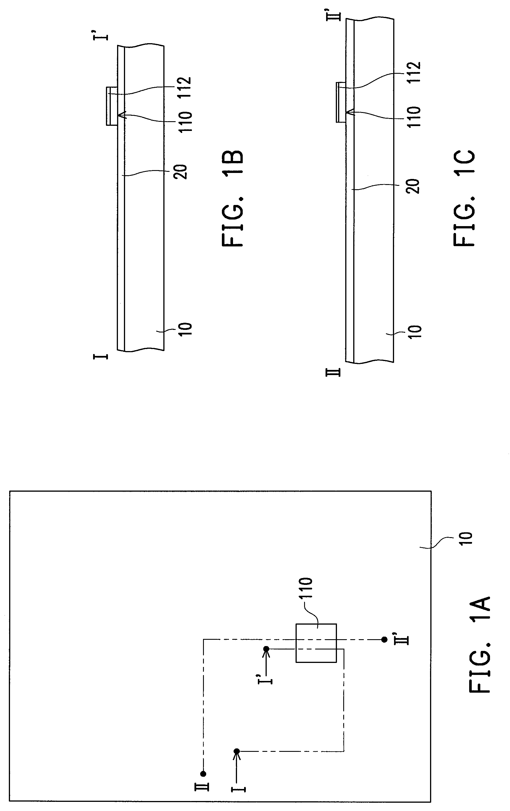
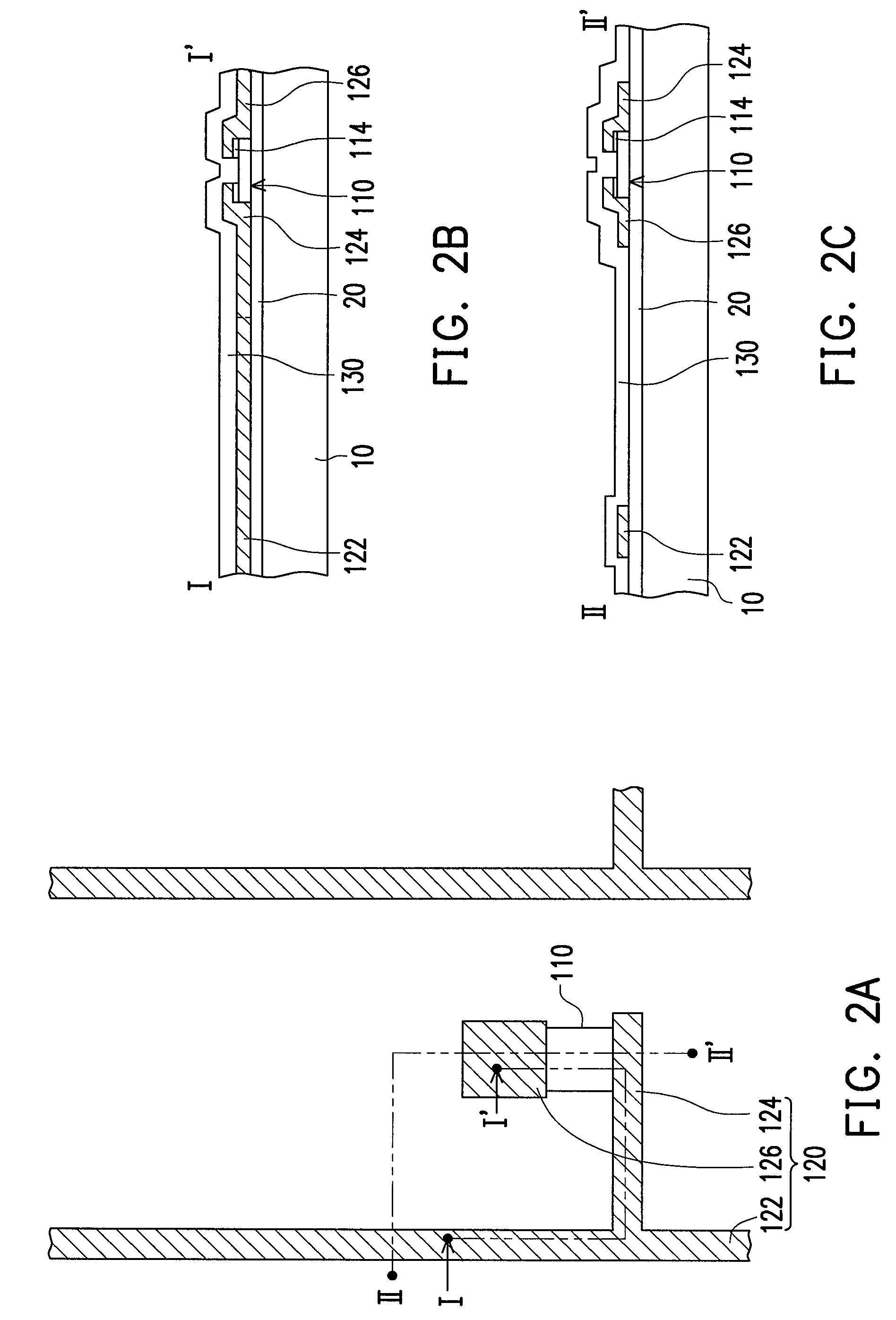
[0038]FIG. 1A is a schematic top view illustrating a fabrication method of a pixel structure with use of a first photomask according to an embodiment of the invention. FIG. 1B and FIG. 1C are respectively cross-sectional views taken along section lines I-I′ and II-II′ depicted in FIG. 1A. With reference to FIG. 1A, FIG. 1B, and FIG. 1C, in the fabrication method described in the present embodiment, a channel layer 110 is formed on a substrate 10. The channel layer 110 may be formed with use of the first photomask. Namely, in this step, a layer of semiconductor material is formed on the substrate 10 by performing a physical vapor deposition (PVD) process, a chemical vapor deposition (CVD) process, a sputtering process, or the like deposition process. A photolithography and an etching processes are performed with use of a first photomask (not shown), so as to pattern the layer of semiconductor material and to form the channel layer 110.

[0039]According to the present embodiment of the ...


PUM

PropertyMeasurementUnit
semiconductoraaaaaaaaaa
widthaaaaaaaaaa
voltageaaaaaaaaaa

Abstract

A pixel structure and its fabrication method are provided. The pixel structure includes a channel layer, a first patterned metal layer, a first insulation layer, a second patterned metal layer, a second insulation layer, and a pixel electrode. The first patterned metal layer includes a data line, a source, and a drain. The first insulation layer has a first opening exposing the drain. The second patterned metal layer includes a scan line and a capacitor electrode. The capacitor electrode has at least one first portion overlapping the data line. The second insulation layer has a second opening communicating with the first opening to expose the drain. The pixel electrode is connected to the drain through the first opening and the second opening and at least overlaps the first portion of the capacitor electrode.

Description

CROSS-REFERENCE TO RELATED APPLICATION[0001]This application claims the priority benefit of Taiwan application serial no. 100141606, filed on Nov. 15, 2011. The entirety of the above-mentioned patent application is hereby incorporated by reference herein and made a part of this specification.BACKGROUND OF THE INVENTION[0002]1. Field of the Invention[0003]The invention relates to a pixel structure and a fabrication method of the pixel structure. More particularly, the invention relates to both a pixel structure that has a high aperture ratio and can be easily fabricated and a fabrication method of the pixel structure.[0004]2. Description of Related Art[0005]In general, a pixel structure of a liquid crystal display (LCD) includes active devices and pixel electrodes. The active devices serve as switches of LCD display units. To control each pixel structure, a certain pixel is usually selected by a corresponding scan line and a corresponding data line, and display information correspond...

Claims


Application Information

Patent Timeline
Patent Type & Authority Patents(United States)
IPC IPC(8): H01L29/10H01L29/04H01L31/00
CPCG02F1/1368H01L27/1255G02F1/136213G02F2001/13685H01L27/1225G02F1/13685
Inventor HUANG, CHANG-YUCHEN, PEI-MING
Owner AU OPTRONICS CORP
Why Eureka
Try Eureka