Semiconductor device and method for producing same

Active Publication Date: 2015-02-12
SHARP KK
View PDF5 Cites 2 Cited by
  • Summary
  • Abstract
  • Description
  • Claims
  • Application Information

AI Technical Summary

Benefits of technology

[0028]An embodiment of the present invention provides a TFT substrate which can be fabricated by a simpler process and which can contribute to realizing a

Problems solved by technology

Recently, as the definition of liquid crystal display devices and other devices has become higher and higher, a decrease in pixel aperture ratio has become an increasingly serious problem.
On top of that, if the aperture ratio

Method used


Image

  • Semiconductor device and method for producing same
  • Semiconductor device and method for producing same
  • Semiconductor device and method for producing same

Examples


Example

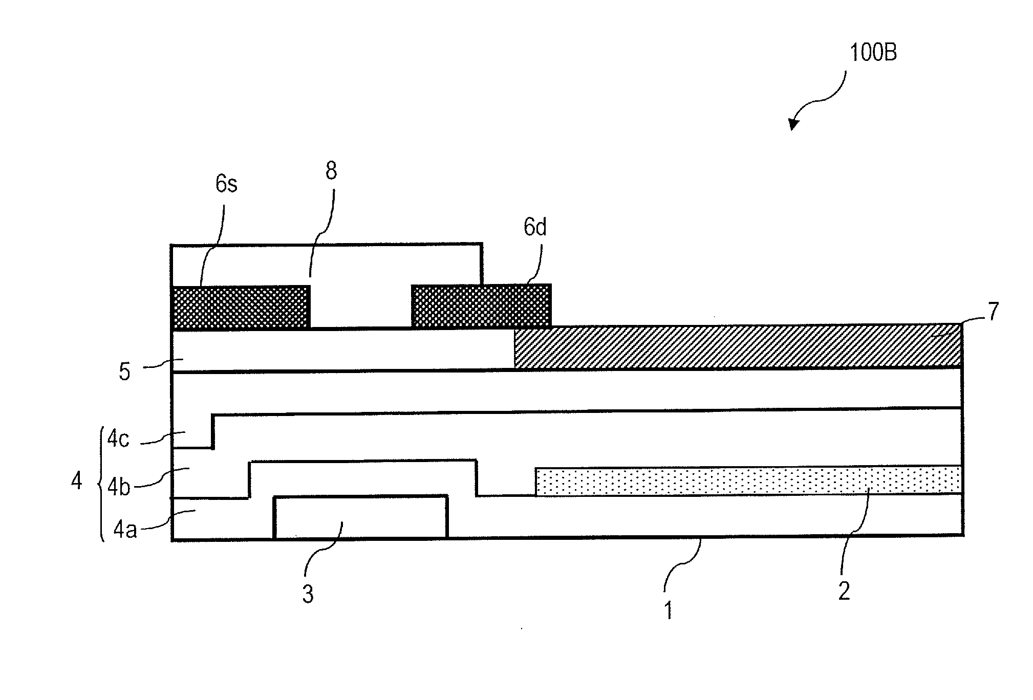
[0035]Hereinafter, a semiconductor device according to an embodiment of the present invention will be described with reference to the accompanying drawings. A semiconductor device according to this embodiment includes a thin-film transistor which has an active layer made of an oxide semiconductor (and which will be referred to herein as an “oxide semiconductor TFT”). A semiconductor device according to this embodiment just needs to include an oxide semiconductor TFT and may be implemented broadly as an active-matrix substrate or any of various kinds of display devices and electronic devices.

[0036]In the following description, a semiconductor device according to an embodiment of the present invention will be described as being applied to an oxide semiconductor TFT for use in a liquid crystal display device.

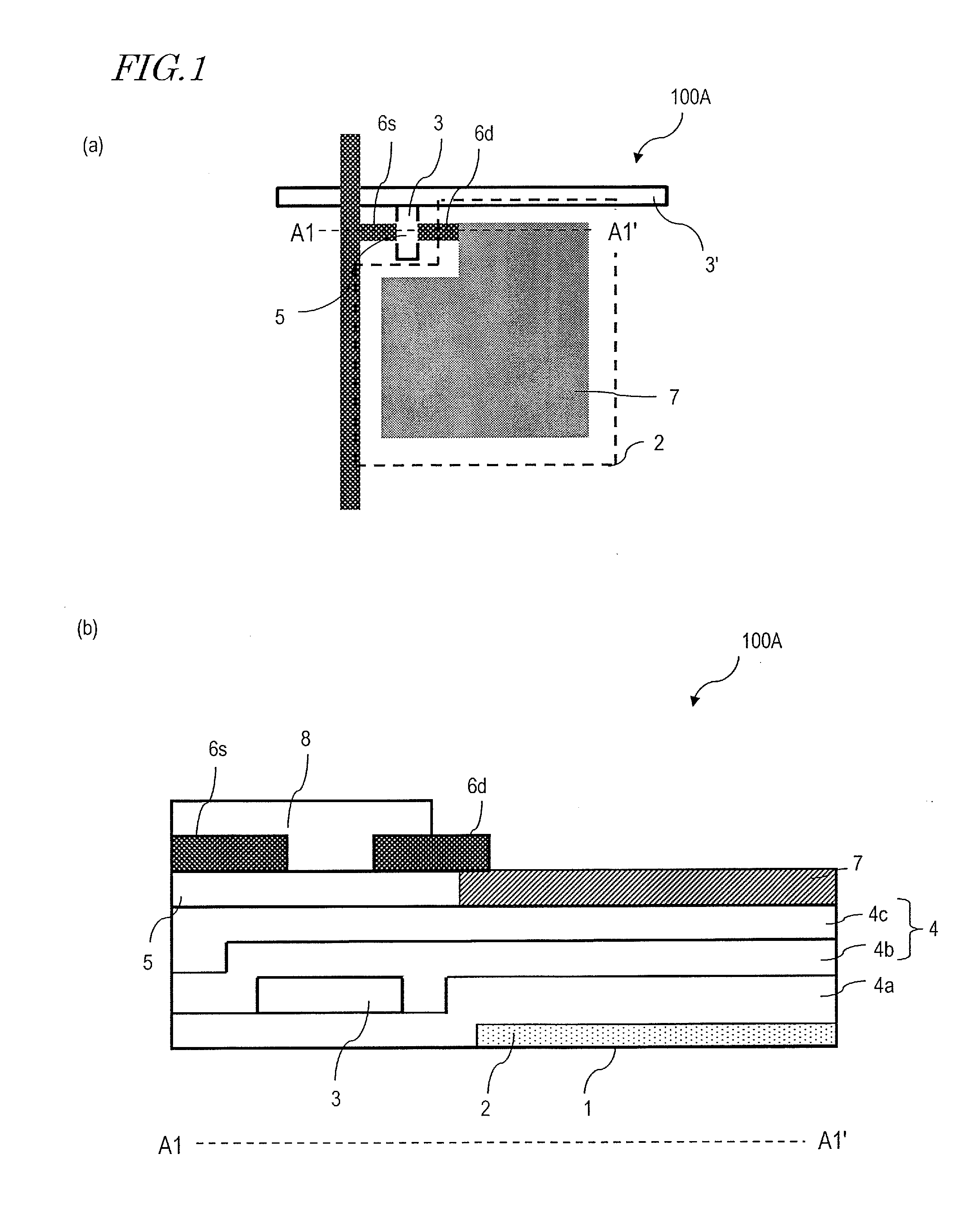
[0037]FIG. 1(a) is a schematic plan view illustrating a TFT substrate 100A according to this embodiment. FIG. 1(b) is a schematic cross-sectional view of the semiconductor device (...


PUM


Abstract

This semiconductor device (100A) includes: a substrate (1); a gate electrode (3) and a first transparent electrode (2) which are formed on the substrate (1); a first insulating layer (4) formed over the gate electrode (3) and the first transparent electrode (2); an oxide semiconductor layer (5) formed on the first insulating layer (4); source and drain electrodes (6s, 6d) electrically connected to the oxide semiconductor layer (5); and a second transparent electrode (7) electrically connected to the drain electrode (6d). At least a portion of the first transparent electrode (2) overlaps with the second transparent electrode (7) with the first insulating layer (4) interposed between them, and the oxide semiconductor layer (5) and the second transparent electrode (7) are formed out of the same oxide film.

Description

TECHNICAL FIELD[0001]The present invention relates to a semiconductor device which has been formed using an oxide semiconductor and a method for fabricating such a device, and more particularly relates to an active-matrix substrate for use in a liquid crystal display device or an organic EL display device and a method for fabricating such a substrate. In this description, the “semiconductor devices” include an active-matrix substrate and a display device which uses the active-matrix substrate.BACKGROUND ART[0002]An active-matrix substrate for use in a liquid crystal display device and other devices includes switching elements such as thin-film transistors (which will be simply referred to herein as “TFTs”), each of which is provided for an associated one of pixels. An active-matrix substrate including TFTs as switching elements is called a “TFT substrate”.[0003]As for TFTs, a TFT which uses an amorphous silicon film as its active layer (and will be referred to herein as an “amorphou...

Claims


Application Information

Patent Timeline
IPC IPC(8): H01L29/786H01L29/45H01L29/66H01L27/12
CPCH01L29/7869H01L27/1225H01L27/1259H01L29/66969H01L29/45G02F1/1368H01L29/4908H01L29/78693G02F2202/10G02F2201/40
Inventor MIYAMOTO, TADAYOSHIITO, KAZUATSUMORI, SHIGEYASUMIYAMOTO, MITSUNOBUOGAWA, YASUYUKINAKAZAWA, MAKOTOUCHIDA, SEIICHIMATSUO, TAKUYA
Owner SHARP KK
Why Eureka
Try Eureka