Modelling current flows in three-dimensional conductive and dielectric bodies

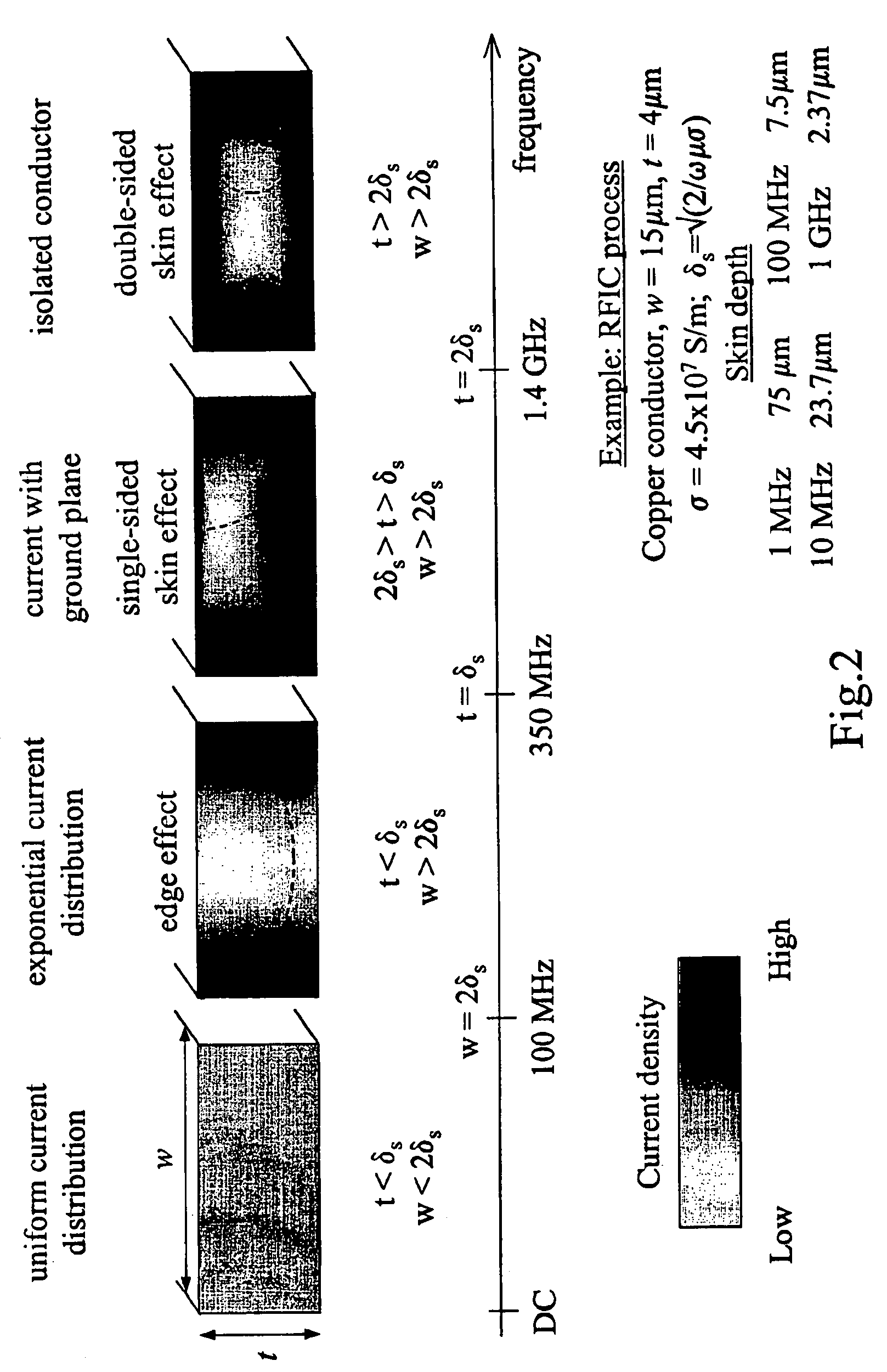
a technology of conductive and dielectric bodies and current flows, applied in the field of model only providing good, infinitely thin conductor approximation is not justified for on-chip interconnection, infinitely thin conductor approximation is no longer valid,

Active Publication Date: 2008-02-12
KEYSIGHT TECH
View PDF9 Cites 11 Cited by
  • Summary
  • Abstract
  • Description
  • Claims
  • Application Information

AI Technical Summary

Benefits of technology

[0057]The invention can be used not only for finite conductors but also to handle the presence of finite dielectrics. An advantage of the invention is that it also restores the planar stratified nature of the background medium, such that the Green's functions GA(r,r′) and GV(r,r′) can still be used without modification.
is that it also restores the planar stratified nature of the background medium, such that the Green's functions GA(r,r′) and GV(r,r′) can still be used without modification.

Problems solved by technology

However, at high frequencies the model only provides good results when applied for good conductors, much wider than their thickness (typically w / t>5) and in proximity to the groundplane, so that the HF currents are flowing on one side of the conductor.
However, at high frequencies the model only provides good results when applied for isolated good conductors, much wider than their thickness, so that the HF currents are evenly distributed and flowing both at the top and bottom sides of the conductor.
It is quite clear that the infinitely-thin conductor approximation is not justified for on-chip interconnections.
All these considerations lead to the conclusion that the infinitely-thin conductor approximation is no longer valid and improved modelling of the conductors is required.
However, when applied to 3D planar conductors embedded in a multilayered medium they become numerically very intensive (the discretisation size inside the conductor must typically be smaller than the skin depth) and not practical for real-life structures.
A disadvantage of this approach is that these models are only valid for good conductors which are much wider than their thickness (typically w / t>5).
These assumptions usually lead to an overestimation of the high frequency loss.
The surface impedances used for the top and bottom layer are however uncoupled and do not account for the mutual internal inductance.
As already outlined above, planar EM solvers approximate the problem by introducing a scalar surface impedance that becomes inaccurate for thick conductors and is not suited for dielectrics.
This approach has two major disadvantages when used in conjunction with a planar EM solver:The need to introduce both equivalent electric and magnetic surface currents doubles the number of unknowns that have to be handled by the solver as compared to the case where only electric surface currents are needed.Present planar solver technology is inherently based on the concept that a conductor surface is modelled by electric surface currents alone.

Method used


Image

  • Modelling current flows in three-dimensional conductive and dielectric bodies
  • Modelling current flows in three-dimensional conductive and dielectric bodies
  • Modelling current flows in three-dimensional conductive and dielectric bodies

Examples


Embodiment Construction

[0077]For convenience an example implementation of the invention will be described in the context of electronic circuit design, using apparatus as shown in FIG. 8 for simulating operation of an electronic circuit.

[0078]Referring to FIG. 8, the apparatus comprises a processing unit 10 and a user input / output interface unit 12. The processing unit 10 includes a central processing unit (CPU), random-access memory (RAM), hard disc storage and associated circuitry to enable the CPU to implement procedures in accordance with software program instructions stored in the RAM, and to interact with the interface unit 12 to receive input from the user and display the results of the procedures. The interface unit 12 typically comprises a visual-display unit (VDU), keyboard, mouse and / or tablet or similar pointing device, and a printer or other hard-copy output device.

[0079]In preparing to perform a system simulation, the apparatus receives, via the interface unit 12, a physical description of th...


PUM

PropertyMeasurementUnit
lengthaaaaaaaaaa
thicknessaaaaaaaaaa
frequenciesaaaaaaaaaa

Abstract

Current flows in a three-dimensional conductive or dielectric body embedded in a substrate of a different material are modelled in terms of surface currents induced in planar surfaces bounding the body and composed of the same material as the substrate, the surfaces having appropriate values for surface impedance.

Description

[0001]This application claims priority from United Kingdom Patent Application No. 0404624.9, filed on 24 Mar. 2004, which is incorporated by reference in its entirety.[0002]This invention relates to methods and apparatus for modelling current flows in three-dimensional conductive and dielectric bodies, for example finite thickness conductors in planar electromagnetic circuit simulations.BACKGROUND ART[0003]Planar electromagnetic (EM) simulation technology enables, in generalised terms, the modelling of three-dimensional electromagnetic fields excited by currents flowing in planar conductors embedded in a multilayered dielectric medium. In this technology, planar conductors that are actually three-dimensional (i.e. have a thickness that is not negligible in terms of circuit operation relative to their width) are approximated as zero thickness sheet conductors. These conductors are treated as being printed on or embedded in a stratified dielectric layer stack (also called the substrat...

Claims


Application Information

Patent Timeline
Patent Type & Authority Patents(United States)
IPC IPC(8): G06F17/50
CPCG06F17/5036G06F30/367
Inventor SERCU, JEANNICKVAN HESE, JANDE ZUTTER, DANIELKNOCKAERT, LUC
Owner KEYSIGHT TECH
Why Eureka
Try Eureka