

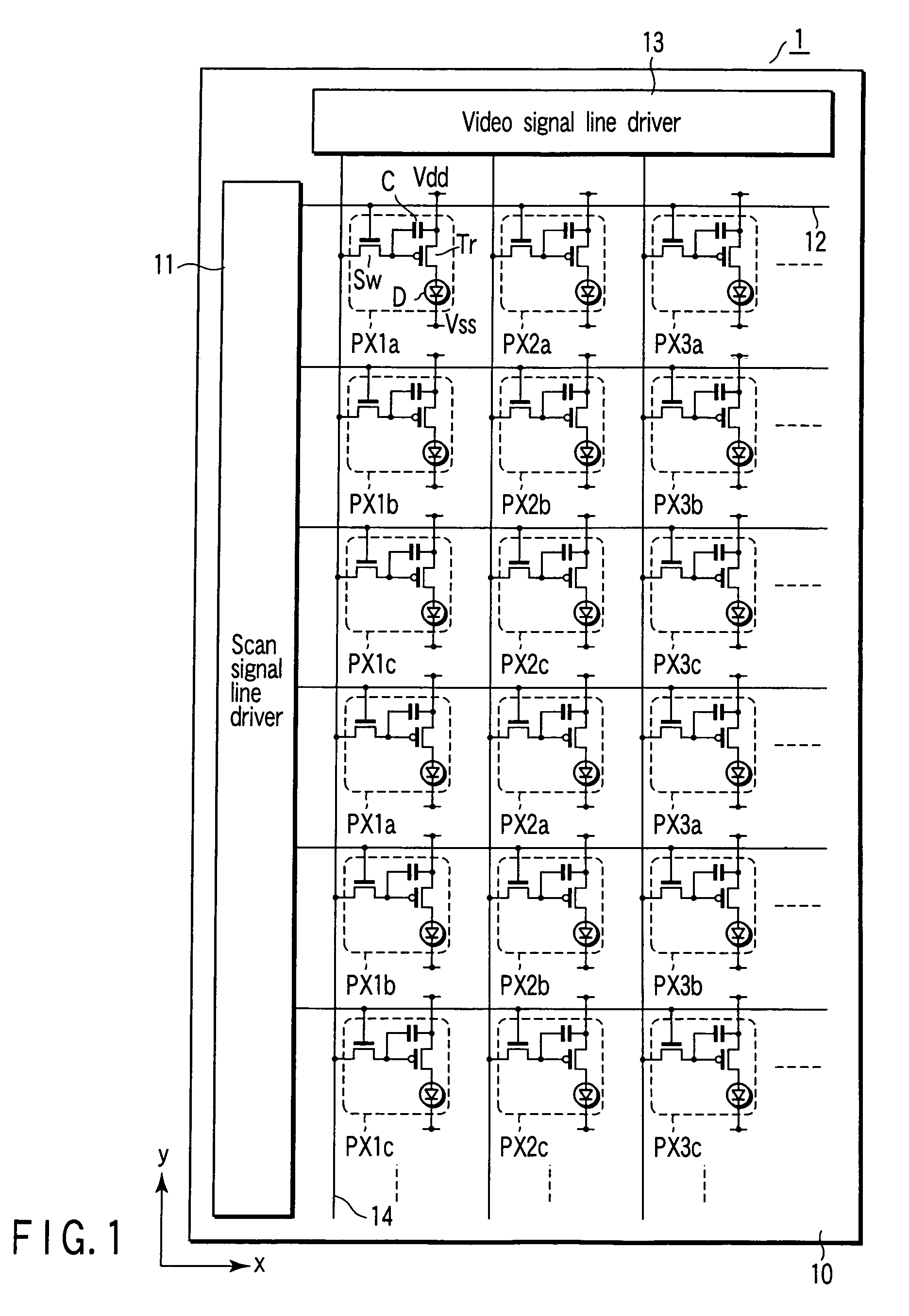
Active matrix display and method of manufacturing the same
a technology of active matrix and display, which is applied in the direction of identification means, instruments, static indicating devices, etc., can solve the problem that display irregularities tend to be visually recognized
- Summary
- Abstract
- Description
- Claims
- Application Information
AI Technical Summary
Benefits of technology
Problems solved by technology
Method used
Image

Examples
example
[0054]FIGS. 6 to 11 are sectional views showing a n example of a method which can be used for the manufacture of the display shown in FIG. 1.
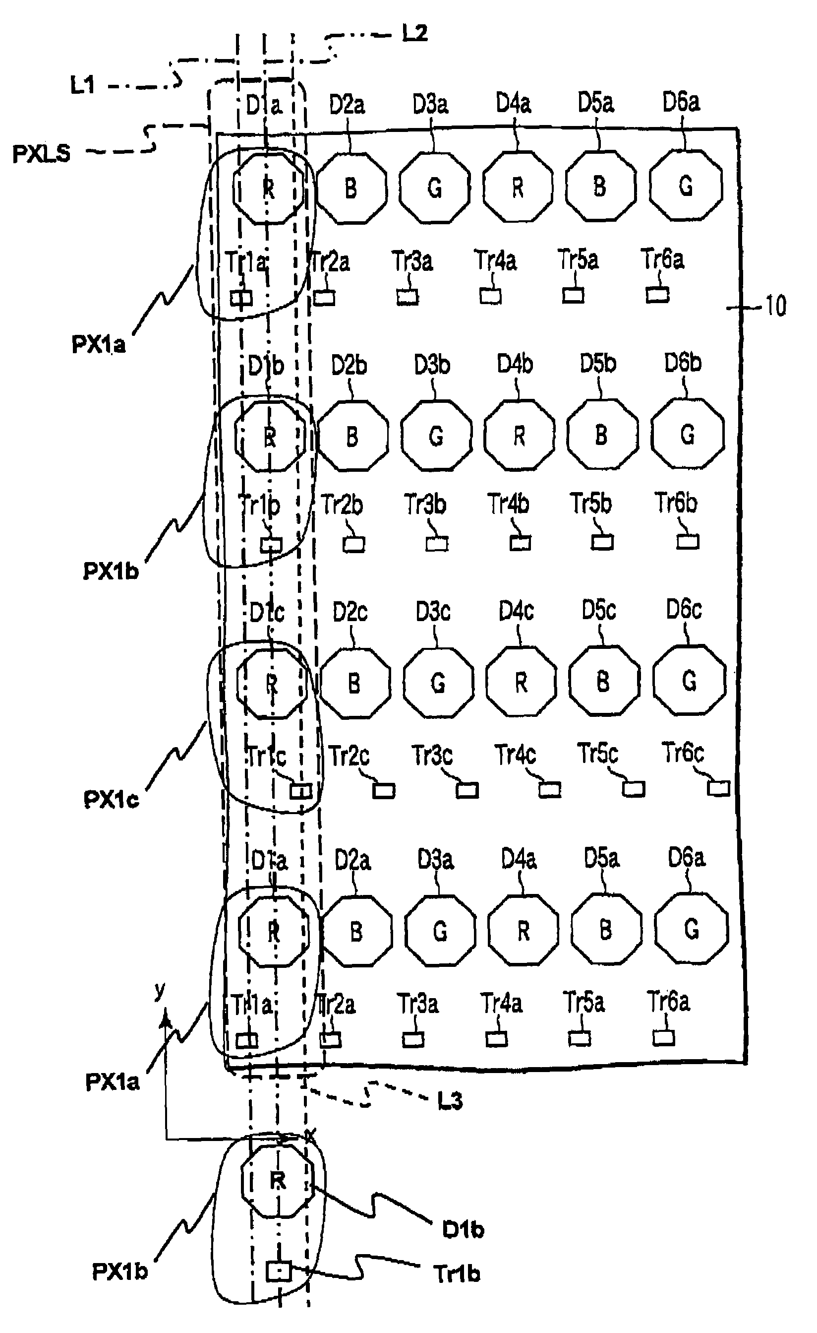
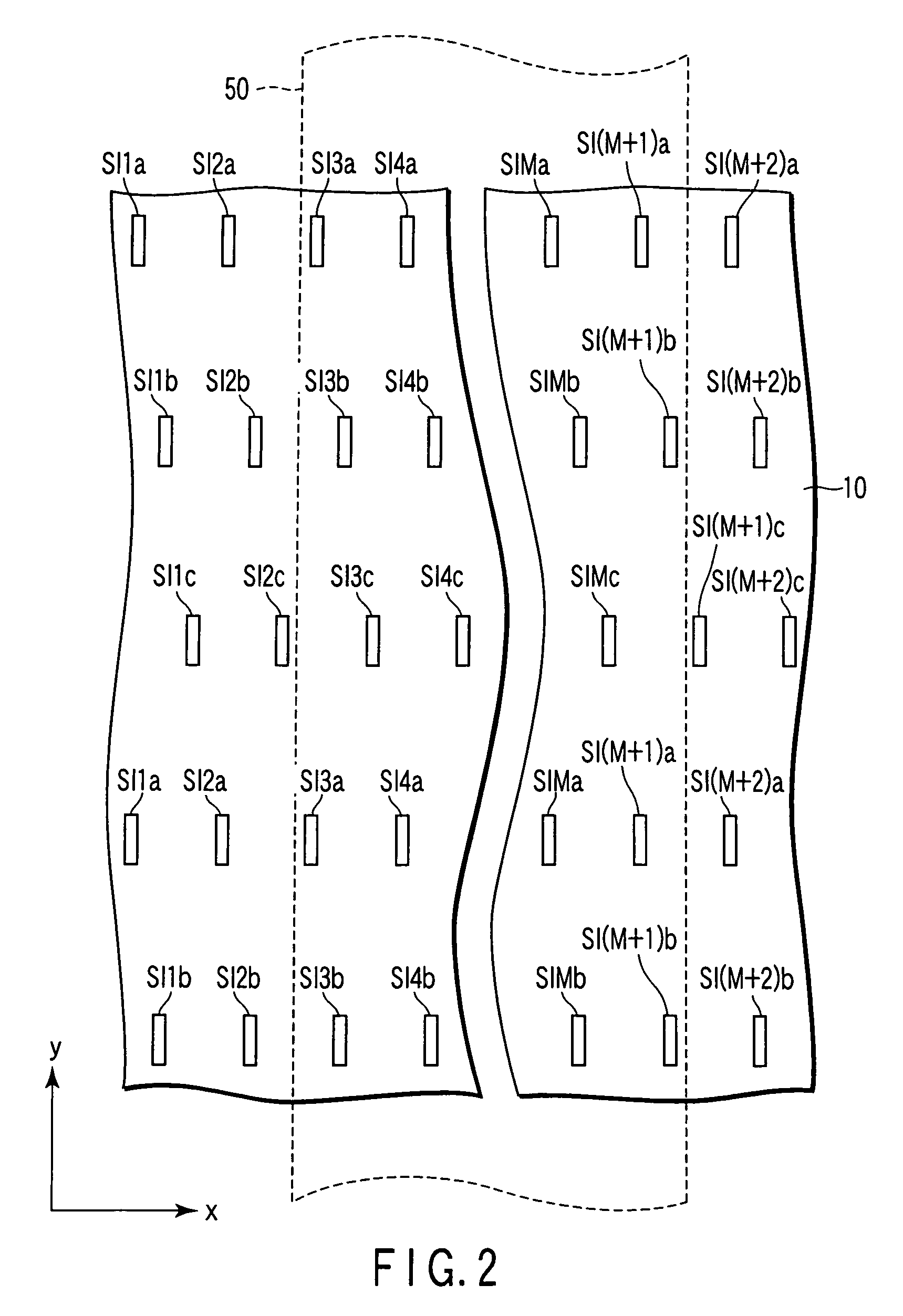
[0055]In this case, an organic EL display 1 shown in FIG. 1 was manufactured by the method to be described below with reference to FIGS. 6 to 11. Note that in the organic EL display 1, the arrangement shown in FIG. 2 is adopted for transistor formation portions SI and the arrangement shown in FIG. 4 is adopted for organic EL elements D and drive transistors Tr.
[0056]After, for example, an SiNx layer 25 and SiO2 layer 26 were formed as undercoat layers on a glass substrate 10, an amorphous silicon layer having a thickness of about 50 nm was formed on the resultant structure. The amorphous silicon layer was then formed into a polysilicon layer by performing laser annealing using, for example, an XeCl excimer laser. The polysilicon layer was patterned to leave a portion corresponding to the transistor formation portion SI shown in FIG. 2, thereby ...
PUM
| Property | Measurement | Unit |
|---|---|---|
| thickness | aaaaa | aaaaa |
| length | aaaaa | aaaaa |
| length | aaaaa | aaaaa |
Abstract
Description
Claims
Application Information