
Active matrix display and method of manufacturing the same

a technology of active matrix and display, which is applied in the direction of identification means, instruments, static indicating devices, etc., can solve the problem that display irregularities tend to be visually recognized

Active Publication Date: 2005-06-02
JAPAN DISPLAY CENTRAL CO LTD
View PDF6 Cites 4 Cited by
  • Summary
  • Abstract
  • Description
  • Claims
  • Application Information

AI Technical Summary

Benefits of technology

[0013] It is an object of the present invention to provide an active matrix display whose display irregularity is hard to recognize and a method of manufacturing the same.

Problems solved by technology

In such an active matrix display, however, display irregularity tends to be visually recognized due to variations in the characteristics of the polysilicon thin film transistors among the respective pixels.

Method used


Image

  • Active matrix display and method of manufacturing the same
  • Active matrix display and method of manufacturing the same
  • Active matrix display and method of manufacturing the same

Examples


example)

(EXAMPLE)

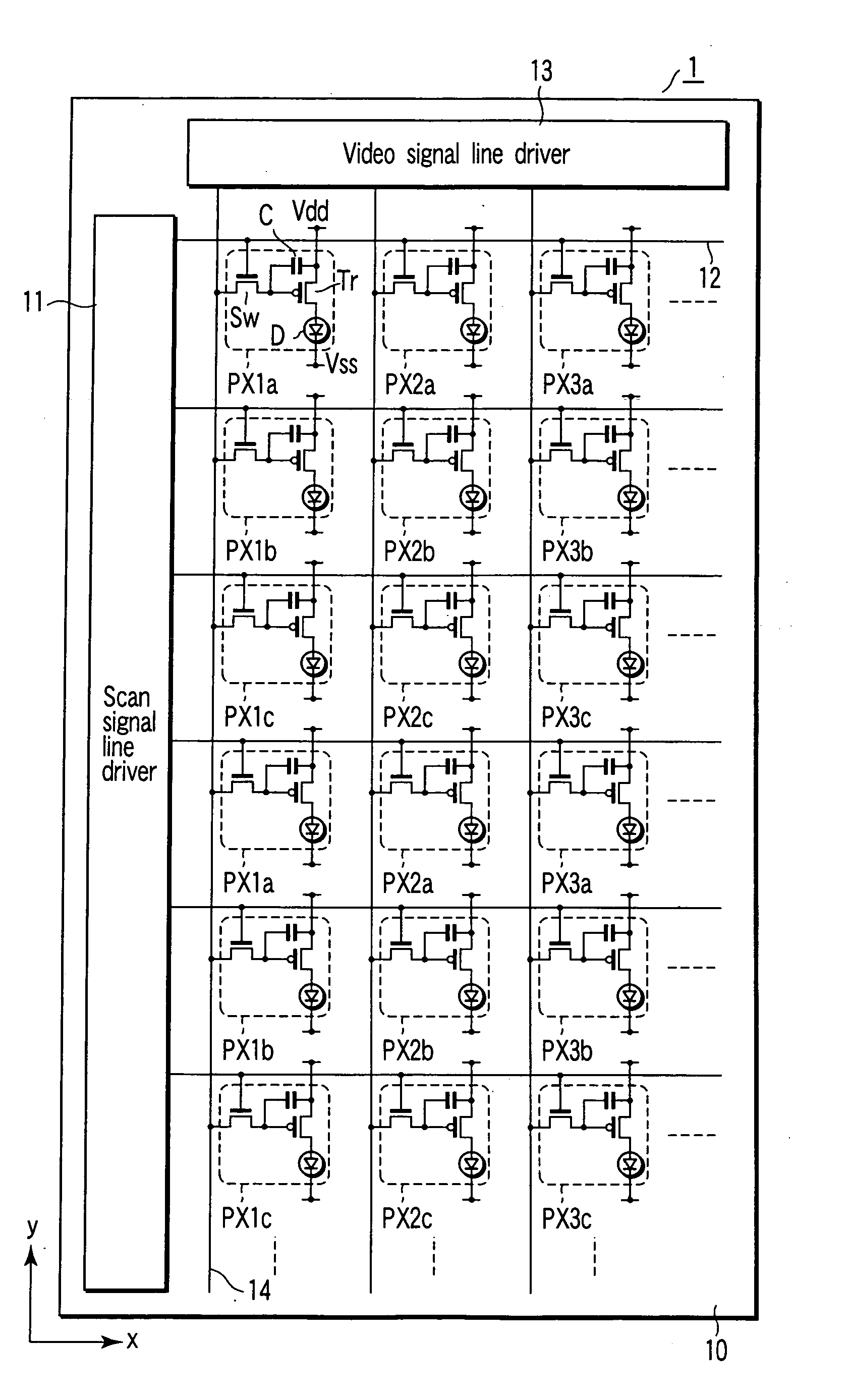
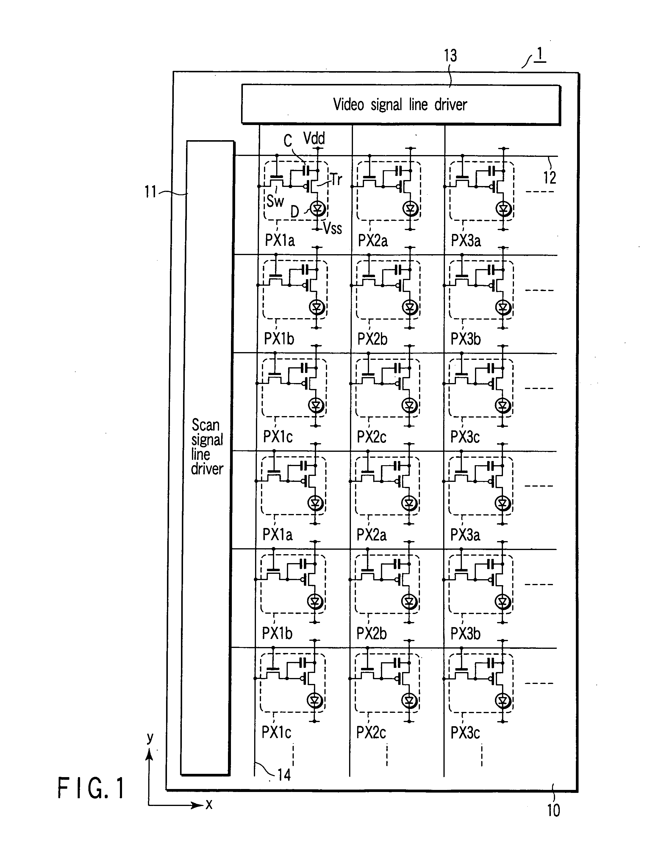
[0053] FIGS. 6 to 11 are sectional views showing an example of a method which can be used for the manufacture of the display shown in FIG. 1.

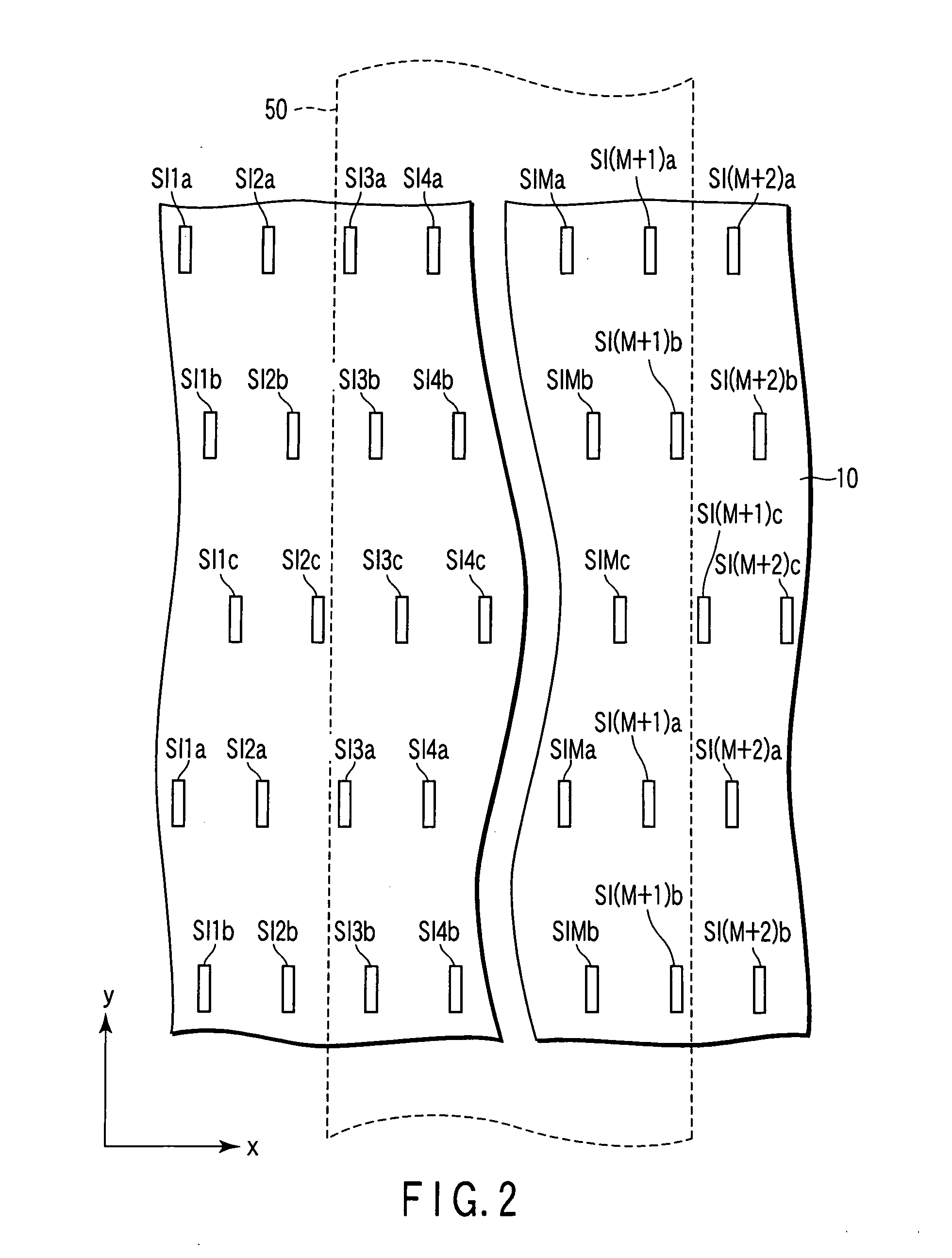
[0054] In this case, an organic EL display 1 shown in FIG. 1 was manufactured by the method to be described below with reference to FIGS. 6 to 11. Note that in the organic EL display 1, the arrangement shown in FIG. 2 is adopted for transistor formation portions SI and the arrangement shown in FIG. 4 is adopted for organic EL elements D and drive transistors Tr.

[0055] After, for example, an SiNx layer 25 and SiO2 layer 26 were formed as undercoat layers on a glass substrate 10, an amorphous silicon layer having a thickness of about 50 nm was formed on the resultant structure. The amorphous silicon layer was then formed into a polysilicon layer by performing laser annealing using, for example, an XeCl excimer laser. The polysilicon layer was patterned to leave a portion corresponding to the transistor formation portion SI shown in FIG...


PUM

PropertyMeasurementUnit
thicknessaaaaaaaaaa
lengthaaaaaaaaaa
lengthaaaaaaaaaa

Abstract

There is provided an active matrix display including pixels arrayed in a matrix form and each including a display element and a thin film transistor. In each of columns which the pixels form, the pixels are divided into a first pixel group in which the thin film transistors are arranged along a first straight line parallel with the column, and a second pixel group in which the thin film transistors are arranged along a second straight line parallel with the column and spaced apart from the first straight line.

Description

CROSS-REFERENCE TO RELATED APPLICATIONS [0001] This application is based upon and claims the benefit of priority from prior Japanese Patent Application No. 2003-400612, filed Nov. 28, 2003, the entire contents of which are incorporated herein by reference. BACKGROUND OF THE INVENTION [0002] 1. Field of the Invention [0003] The present invention relates to an active matrix display and a manufacturing method thereof. [0004] 2. Description of the Related Art [0005] Displays such as light-emitting diode displays and liquid crystal displays have advantageous characteristics such as decreased thickness. For this reason, these displays have been used for office equipment, computers, and the like. Recently, organic EL (Electro-Luminescent) displays have been developed, which are superior to liquid crystal displays in the following points. [0006] 1) An organic EL display is bright and self-emissive, and hence can realize a bright and clear display, a wide viewing angle, and reductions in pow...

Claims


Application Information

Patent Timeline
Patent Type & Authority Applications(United States)
IPC IPC(8): G02F1/1368G02F1/1345G09F9/00G09F9/30G09G3/30H01L21/336H01L29/786H01L51/50H05B33/00H05B33/10H05B33/12H05B33/14H05B44/00
CPCG09G3/3208G09G2320/0233G09G2300/08G09G2300/0426H05B33/00H05B33/10
Inventor GOTO, YASUMASA
Owner JAPAN DISPLAY CENTRAL CO LTD
Learn More