Structure of dielectric layers in built-up layers of wafer level package

a technology of built-up layers and dielectric layers, which is applied in the direction of electrical equipment, semiconductor devices, semiconductor/solid-state device details, etc., can solve problems such as dielectric layer cracks, and achieve the effect of reducing stress accumulation and improving mechanical reliability of wlp

Inactive Publication Date: 2008-11-18
ADVANCED CHIP ENG TECH INC
View PDF2 Cites 32 Cited by
  • Summary
  • Abstract
  • Description
  • Claims
  • Application Information

AI Technical Summary

Benefits of technology

[0010]The present invention provides a structure of elastic dielectric layers with certain open through holes of WLP to absorb the stress. The CTE difference between a RDL and a dielectric layer may cause the dielectric layer crack. To solve this problem, the present invention utilizes elastic dielectric layers; wherein the material of the elastic dielectric layer comprises silicone based material, for example, SINR, PCB, PI, with specific range of CTE, elongation rate and hardness. The elastic dielectric layer can improve the mechanical reliability of the structure of WLP during temperature cycling test. The present invention further provides a structure of dielectric layers with certain open through holes adjacent to the curve of a RDL of a WLP which can reduce the stress accumulated at area of the dielectric layer adjacent to the RDL / dielectric layer interface and then solve the crack problem of the dielectric layer.

Problems solved by technology

The CTE difference between a RDL and a dielectric layer may cause the dielectric layer crack.

Method used


Image

  • Structure of dielectric layers in built-up layers of wafer level package
  • Structure of dielectric layers in built-up layers of wafer level package
  • Structure of dielectric layers in built-up layers of wafer level package

Examples


Embodiment Construction

[0018]The invention will now be described in greater detail with preferred embodiments of the invention and illustrations attached. Nevertheless, it should be recognized that the preferred embodiments of the invention is only for illustrating. Besides the preferred embodiment mentioned here, present invention can be practiced in a wide range of other embodiments besides those explicitly described, and the scope of the present invention is expressly not limited expect as specified in the accompanying claims.

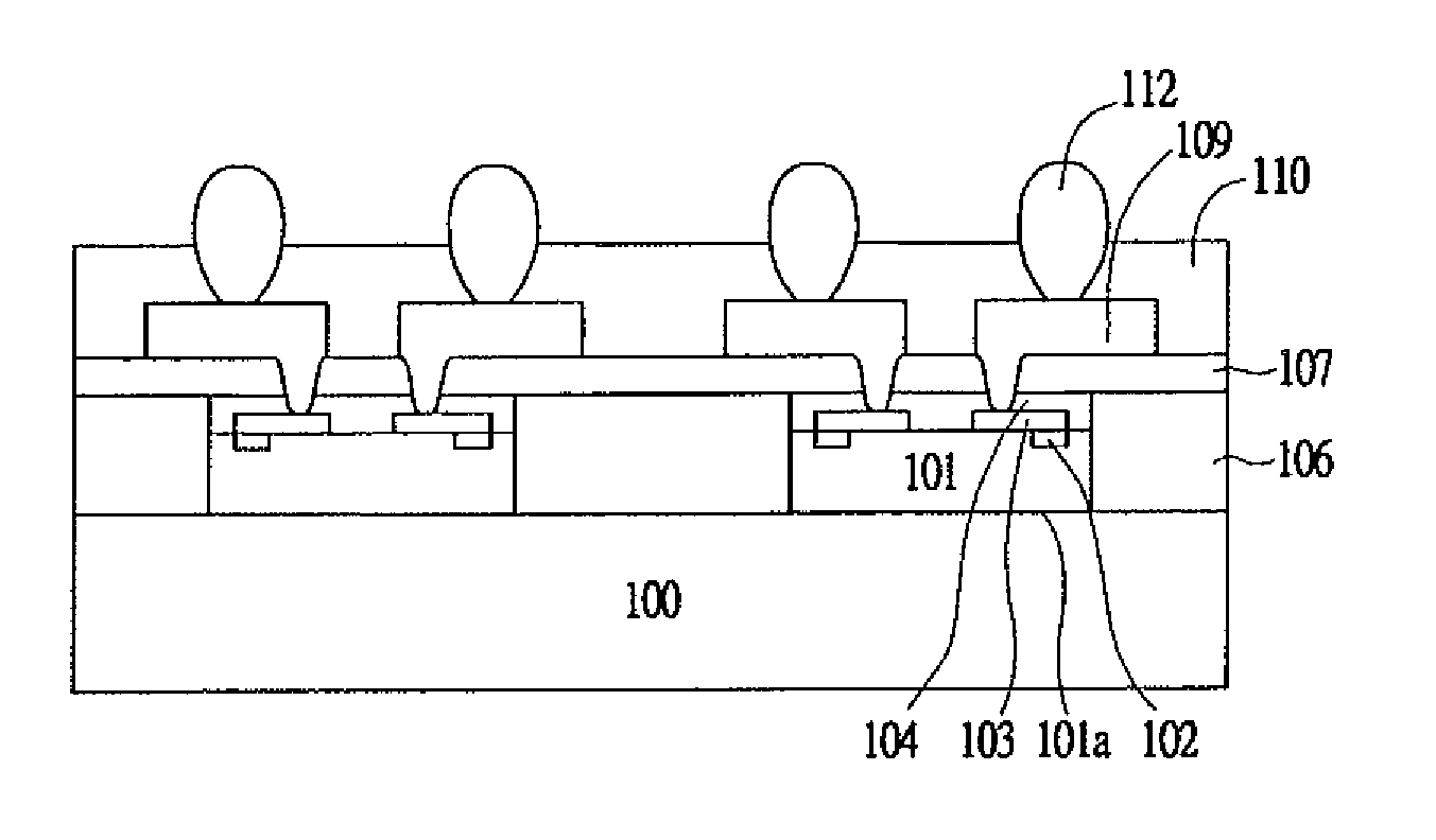
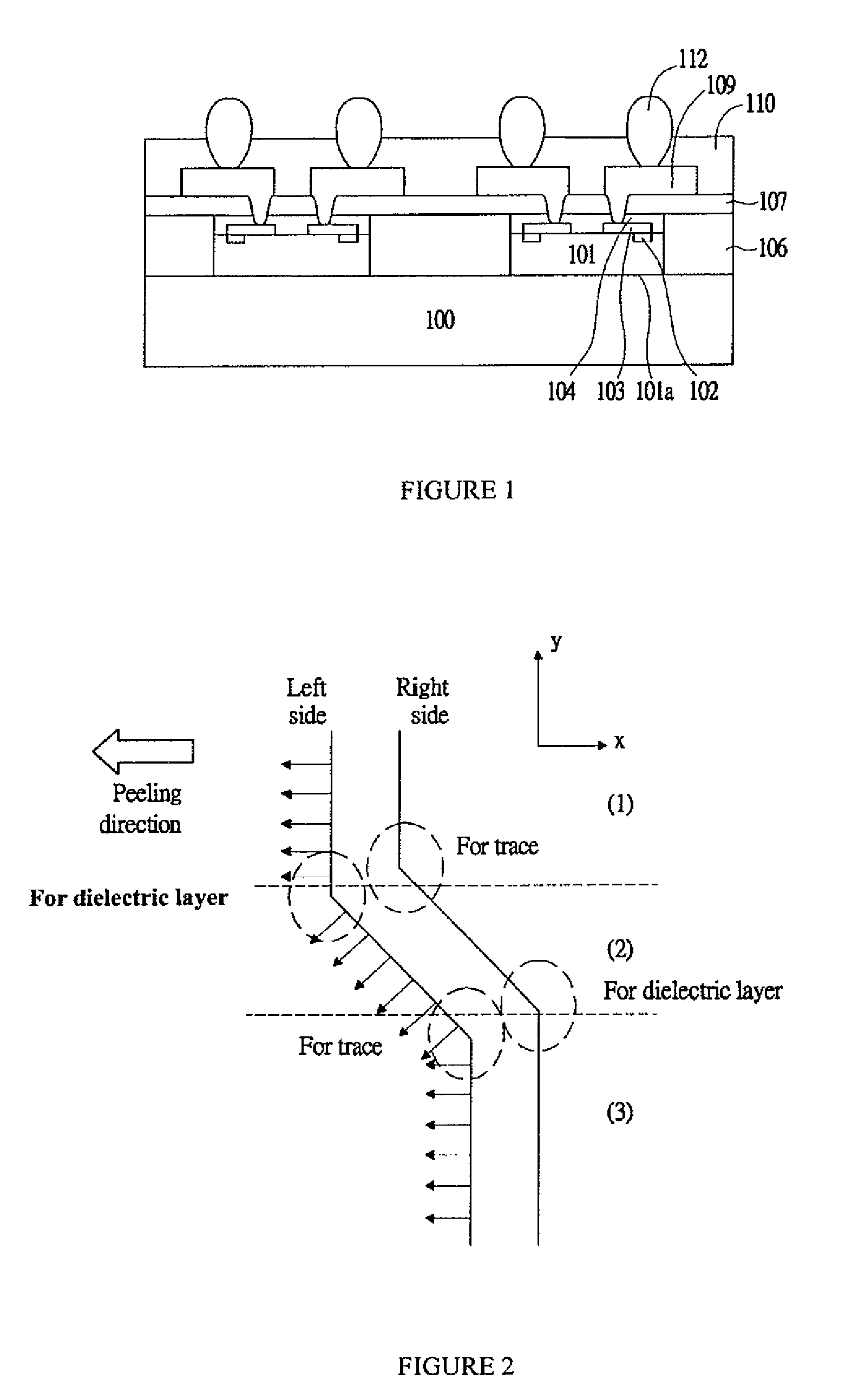
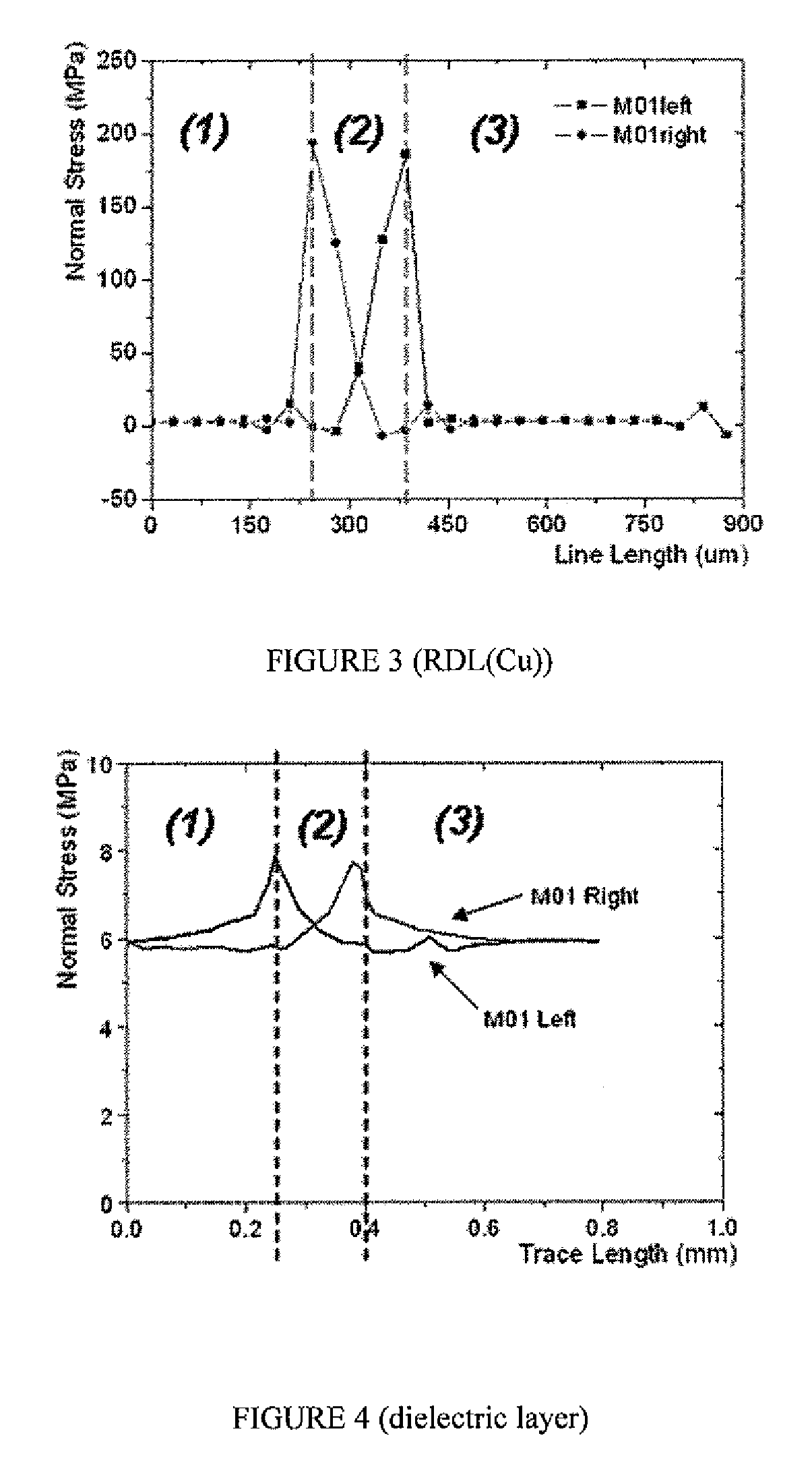
[0019]The present invention discloses a structure of WLP utilizing elastic dielectric layers to improve the mechanical reliability, e.g., absorb the accumulated stress due to CTE mismatching of materials, of the structure of WLP during temperature cycling test. The present invention discloses a structure of the dielectric layer with certain open through holes formed near the curve of the RDL of WLP, by which the stress can be further reduced.

[0020]FIG. 1 illustrates a cross-sectio...


PUM


Abstract

The present invention provides a structure of elastic dielectric layers with certain through holes adjacent to the angle of a RDL of WLP to absorb the stress. The elastic dielectric layer is made from silicone based materials with specific range of CTE, elongation rate and hardness, which can improve the mechanical reliability of the structure during temperature cycling test. The CTE difference between the RDL and the elastic dielectric material still may cause the elastic dielectric layer crack; to solve this problem, The present invention further provides a structure of dielectric layers with certain open through holes adjacent to the curve portion of a RDL of WLP which can reduce the stress accumulated at area of the dielectric layer adjacent to the RDL / dielectric layer interface to solve the crack problem of the dielectric layer.

Description

FIELD OF THE INVENTION[0001]This invention relates to a structure of wafer level package (WLP), and more particularly to a structure of dielectric layers with certain open through holes thereon of WLP.DESCRIPTION OF THE PRIOR ART[0002]For mobile appliances, e.g., cellular phones, notebooks, and the like, or applications where physical space for devices is extremely valuable, e.g., aircraft and the like, size is a critical factor to a successful design of the device, but the demand of reducing the size of a chip conflict with the trend of increasing elements on said chip.[0003]The function of chip package includes power distribution, signal distribution, heat dissipation, protection and support . . . and so on. As a semiconductor become more complicated, the traditional package technique, e.g., lead frame package, flex package, rigid package technique, can't meet the demand of producing smaller chip with high density elements on the chip. Furthermore, because conventional package tec...

Claims


Application Information

Patent Timeline
Patent Type & Authority Patents(United States)
IPC IPC(8): H01L23/48
CPCH01L23/5389H01L24/19H01L2224/73267H01L2224/20H01L2924/01013H01L2924/01029H01L2924/01033H01L2924/01078H01L2924/01079H01L2924/01082H01L2924/14H01L2924/15311H01L2924/01006H01L2924/01075H01L2924/10253H01L2224/04105H01L2924/00H01L2924/351
Inventor YANG, WEN-KUNYU, CHUN-HUICHOU, CHAO-NANLIN, CHIH-WEIHUANG, CHING-SHUN
Owner ADVANCED CHIP ENG TECH INC
Why Eureka
Try Eureka