TFT, electronic device having the TFT, and flat display device having the TFT

a technology of thin film transistors and flat display devices, which is applied in the direction of semiconductor devices, electrical equipment, nanotechnology, etc., can solve the problems of poor electrical reliability, difficult to obtain flexible flat display devices, and more polysilicon, and achieve the effect of facilitating simultaneous formation

Active Publication Date: 2009-08-25
SAMSUNG DISPLAY CO LTD
View PDF10 Cites 12 Cited by
  • Summary
  • Abstract
  • Description
  • Claims
  • Application Information

AI Technical Summary

Benefits of technology

[0015]The present invention provides an improved TFT and a flat display device having such an improved TFT. The structure of the TFT facilitates the simultaneous formation of many different types of TFTs.

Problems solved by technology

However, polysilicon has been more prevalent because amorphous silicon has poor electrical characteristics and low electrical reliability.
Nevertheless, it is difficult to obtain a flexible flat display device when using crystallized polysilicon TFTs formed by a method similar to the one described above.
But these materials, however, do not have high heat resistance.

Method used


Image

  • TFT, electronic device having the TFT, and flat display device having the TFT
  • TFT, electronic device having the TFT, and flat display device having the TFT
  • TFT, electronic device having the TFT, and flat display device having the TFT

Examples


Embodiment Construction

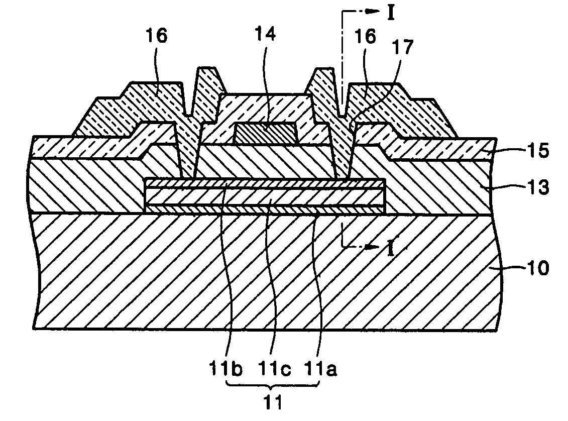
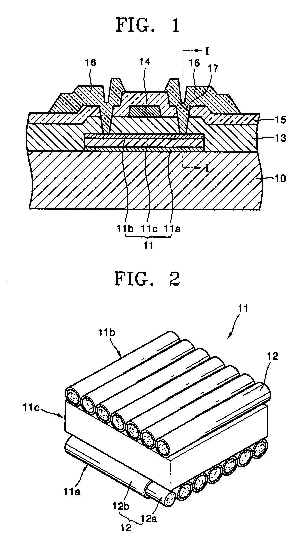
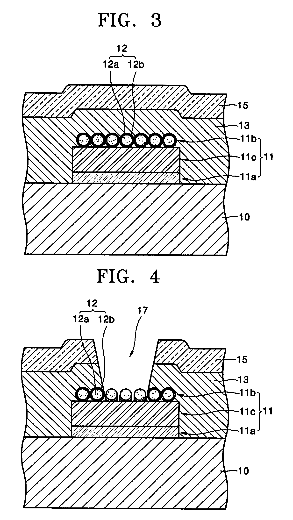
[0033]The present invention will now be described more fully with reference to the accompanying drawings in which embodiments of the invention are shown.

[0034]In the drawings, the thickness of layers and regions are exaggerated for clarity. It will be understood that when an element such as a layer, film, region or substrate is referred to as being “on” another element, it can be directly on the other element or intervening elements may also be present. In contrast, when an element is referred to as being “directly on” another element, there are no intervening elements present. Like numbers refer to like elements throughout the specification.

[0035]Referring to FIG. 1, the TFT is formed on a substrate 10. Substrate 10 may be formed from acryl, polyimide, polycarbonate, polyester, mylar, or plastic, but it is not limited to these materials and can be formed, for example, from a glass material. If necessary, a buffer layer for preventing the diffusion of dopant ions and a barrier layer...


PUM


Abstract

The invention provides an improved thin film transistor (TFT) that can be formed at room temperature and has an improved contact resistance between an active layer and source and drain electrodes, and further provides a flat display device using such a TFT. The TFT includes an active layer including at least two nano particle layers which include at least one nano particle type, an insulating layer interposed between the nano particle layers, a gate electrode insulated from the active layer, and source and drain electrodes formed in respective channels, the source and drain electrodes contact one of the nano particle layers of the active layer. The structure of the TFT facilitates the simultaneous manufacturing of a plurality of different types of TFTs.

Description

CROSS-REFERENCE TO RELATED APPLICATION[0001]This application claims the priority of Korean Patent Application No. 10-2004-0056820, filed on Jul. 21, 2004, in the Korean Intellectual Property Office, the disclosure of which is incorporated by reference in its entirety herein.BACKGROUND OF THE INVENTION[0002]1. Field of the Invention[0003]The present invention relates to a thin film transistor (TFT) and an electronic flat display device having the same, and, in particular, a thin film transistor and an electronic display device including nano particles in at least a channel.[0004]2. Description of the Related Art[0005]Organic electroluminescent display (OELD) devices can be classified as either passive matrix (PM), which uses a manual driving method, or active matrix (AM), which uses an active driving method.[0006]In a PM OELD device, pixels are formed by anode electrodes and cathode electrodes arranged in columns and rows, respectively, whereby scanning signals are supplied to the ca...

Claims


Application Information

Patent Timeline
Patent Type & Authority Patents(United States)
IPC IPC(8): H01L21/00
CPCB82Y10/00H01L27/1214H01L29/78696H01L29/0673H01L29/78681H01L29/0665H01L27/1222H01L27/12
Inventor SUH, MIN-CHULKOO, JAE-BONKIM, HYE-DONG
Owner SAMSUNG DISPLAY CO LTD
Why Eureka
Try Eureka