Supercharge Your Innovation With Domain-Expert AI Agents!

Elastic wave device with stacked piezoelectric substrates

a piezoelectric substrate and elastic wave technology, applied in the direction of impedence networks, electrical devices, etc., to achieve the effect of superior temperature cycle resistivity

Active Publication Date: 2015-09-08
MURATA MFG CO LTD
View PDF27 Cites 4 Cited by
  • Summary
  • Abstract
  • Description
  • Claims
  • Application Information

AI Technical Summary

Benefits of technology

[0006]Preferred embodiments of the present invention provide an elastic wave device having superior temperature cycle resistivity.
[0014]According to various preferred embodiments of the present invention, an elastic wave device having superior temperature cycle resistivity is provided.

Problems solved by technology

However, there is a problem with such an elastic wave device in which a plurality of elastic wave elements are bonded together in an integrated manner having a low temperature cycle resistivity.

Method used


Image

  • Elastic wave device with stacked piezoelectric substrates
  • Elastic wave device with stacked piezoelectric substrates

Examples


first preferred embodiment

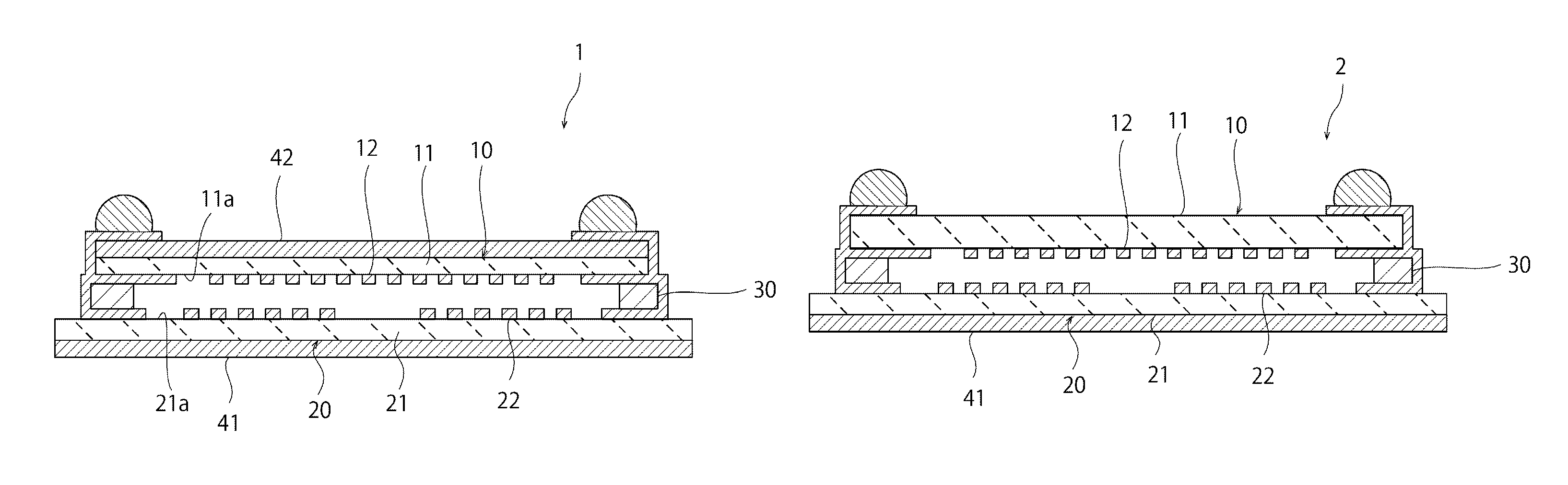
[0020]FIG. 1 is an overall cross-sectional view illustrating an elastic wave device according to a first preferred embodiment of the present invention. As shown in FIG. 1, an elastic wave device 1 includes a first elastic wave element 10 and a second elastic wave element 20. The first elastic wave element 10 includes a first piezoelectric substrate 11 and a first interdigital transducer electrode 12 disposed on one main surface 11a of the first piezoelectric substrate 11. Likewise, the second elastic wave element 20 includes a second piezoelectric substrate 21 and a second interdigital transducer electrode 22 disposed on one main surface 21a of the second piezoelectric substrate 21. The main surface 21a of the second piezoelectric substrate 21 faces the main surface 11a of the first piezoelectric substrate 11. The first and second piezoelectric substrates 11 and 21 are bonded to each other so that the main surfaces 11a and 21a of the first and second piezoelectric substrates 11 and ...

second preferred embodiment

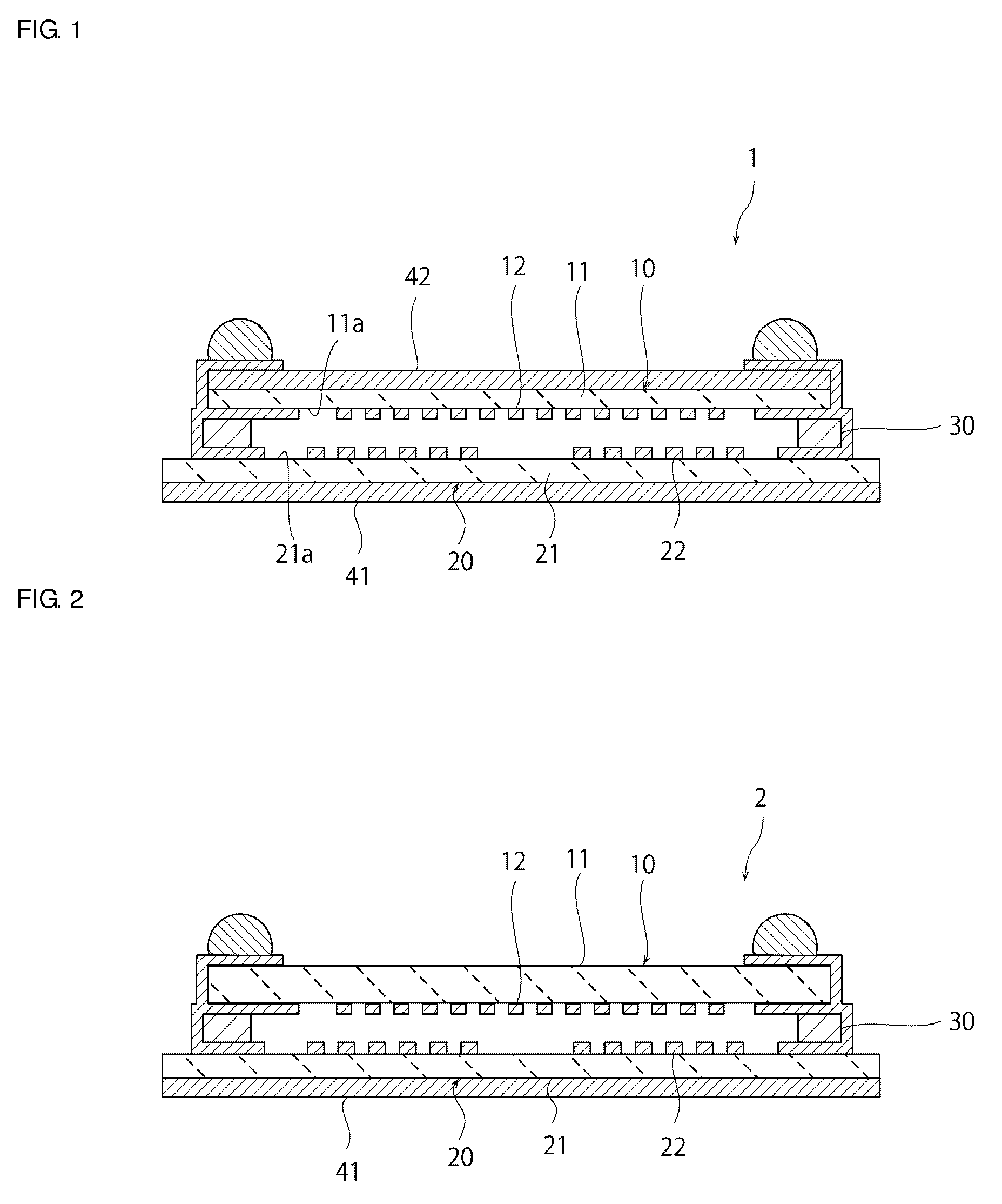
[0030]FIG. 2 is an overall cross-sectional view illustrating an elastic wave device according to a second preferred embodiment of the present invention.

[0031]The first preferred embodiment describes an example of the elastic wave device 1 in which the first substrate 41 is bonded to the second piezoelectric substrate 21 and the second substrate 42 is bonded to the first piezoelectric substrate 11. However, the present invention is not limited to such a configuration.

[0032]For example, the first substrate 41 may be provided and the second substrate 42 may be omitted, as with an elastic wave device 2 shown in FIG. 2. The difference between coefficients of thermal expansion is significantly reduced in this case as well, which makes it possible to realize a superior temperature cycle resistivity.

[0033]Note that in this case, the first substrate 41 preferably is configured of sapphire, silicon, or glass, and / or may have the same composition as the first piezoelectric substrate 11.


PUM


Abstract

An elastic wave device includes a first elastic wave element, a second elastic wave element, and a first substrate. The first elastic wave element includes a first piezoelectric substrate. The second elastic wave element includes a second piezoelectric substrate. The second piezoelectric substrate is stacked on the first piezoelectric substrate. A coefficient of linear expansion of the second piezoelectric substrate is greater than a coefficient of linear expansion of the first piezoelectric substrate. The first substrate is bonded to the second piezoelectric substrate. A coefficient of linear expansion of the first substrate is lower than the coefficient of linear expansion of the second piezoelectric substrate.

Description

BACKGROUND OF THE INVENTION[0001]1. Field of the Invention[0002]The present invention relates to elastic wave devices.[0003]2. Description of the Related Art[0004]Elastic wave devices that use surface acoustic waves, for example, have thus far been widely used in filter devices and the like. Japanese Unexamined Patent Application Publication No. 2011-506106 discloses an elastic wave device in which a plurality of elastic wave elements are bonded together in an integrated manner, for example.[0005]However, there is a problem with such an elastic wave device in which a plurality of elastic wave elements are bonded together in an integrated manner having a low temperature cycle resistivity.SUMMARY OF THE INVENTION[0006]Preferred embodiments of the present invention provide an elastic wave device having superior temperature cycle resistivity.[0007]An elastic wave device according to a preferred embodiment of the present invention includes a first elastic wave element, a second elastic w...

Claims


Application Information

Patent Timeline
Patent Type & Authority Patents(United States)
IPC IPC(8): H03H9/70H03H9/72H03H9/64H03H9/05H03H9/02H03H9/54
CPCH03H9/64H03H9/02834H03H9/0576H03H9/0585H03H9/70H03H9/725H03H9/54H03H9/1092
Inventor KIKUCHI, TAKUYAMAZAKI, HISASHI
Owner MURATA MFG CO LTD
Features
  • R&D
  • Intellectual Property
  • Life Sciences
  • Materials
  • Tech Scout
  • Unparalleled Data Quality
  • Higher Quality Content
  • 60% Fewer Hallucinations
Learn More