Semiconductor device

a technology of semiconductor devices and capacitors, applied in the direction of semiconductor devices, basic electric elements, electrical equipment, etc., to achieve the effect of increasing the feedback capacitance, increasing the capacitance “crss”, and reducing the capacitance between the gate potential

Active Publication Date: 2018-01-02
SHINDENGEN ELECTRIC MFG CO LTD
View PDF25 Cites 0 Cited by
  • Summary
  • Abstract
  • Description
  • Claims
  • Application Information

AI Technical Summary

Benefits of technology

[0032]The so-called feedback capacitance “Crss” is equal to the capacitance “Cgd” between the gate potential and the drain potential, and the so-called input capacitance “Ciss” is equal to the capacitance “Cgd” between the gate potential and the drain potential plus the capacitance “Cgs” between the gate potential and the source potential. In this respect, according to the present invention, the first insulating layers surrounding the first gate electrodes that are at the gate potential are disposed on the opposite sides of the upper end of the column layer that is connected to the source electrode and is at the source potential. In addition, the first insulating layer in contact with the first gate electrode that is at the gate potential is, on the side opposite to the column layer, in contact with the source region and the base layer that are connected to the source electrode and are at the source potential. Therefore, the capacitance “Cgs” between the gate potential and the source potential can be increased without having a significant effect on the capacitance “Cgd” between the gate potential and the drain potential, and therefore, the input capacitance “Ciss” can be increased without significantly increasing the feedback capacitance “Crss”. Therefore, the ratio of the input capacitance “Ciss” to the feedback capacitance “Crss” can be increased, and the possibility that charging and discharging of a capacitance cause the voltage at the gate electrode to increase to lead to malfunction can be reduced.

Problems solved by technology

For example, if two semiconductor devices, such as the MOSFET disclosed in FIG. 15 of Patent Literature 1 described above, are used to achieve synchronous rectification, and the ratio of the input capacitance “Ciss” to the feedback capacitance “Crss” of the semiconductor devices is low, charging and discharging of the capacitances can cause the gate voltage to increase to cause malfunction and turn on a semiconductor device turned off.

Method used


Image

  • Semiconductor device
  • Semiconductor device
  • Semiconductor device

Examples


first embodiment

[0044]>

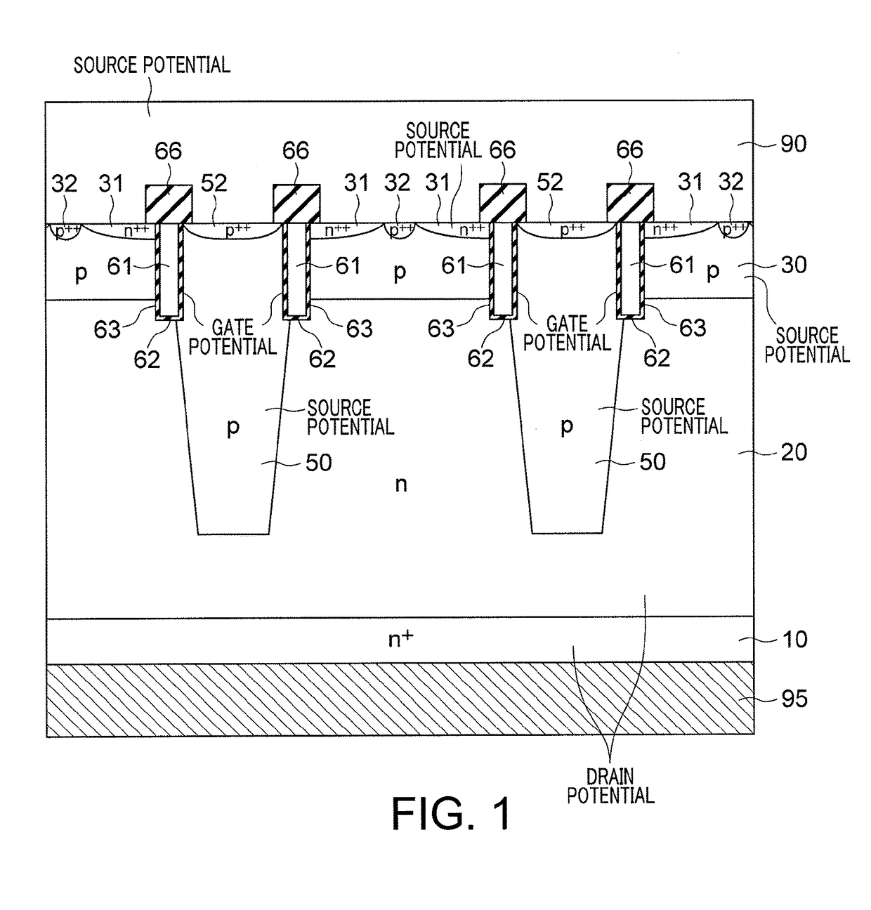
[0045]In the following, a semiconductor device according to a first embodiment of the present invention will be described with reference to the drawings. FIGS. 1 to 3 are diagrams for illustrating the first embodiment of the present invention.

[0046]A semiconductor device according to this embodiment is a vertical power MOSFET, for example. In the following, the semiconductor device will be described as a vertical power MOSFET. However, note that the vertical power MOSFET is only an example of the semiconductor device.

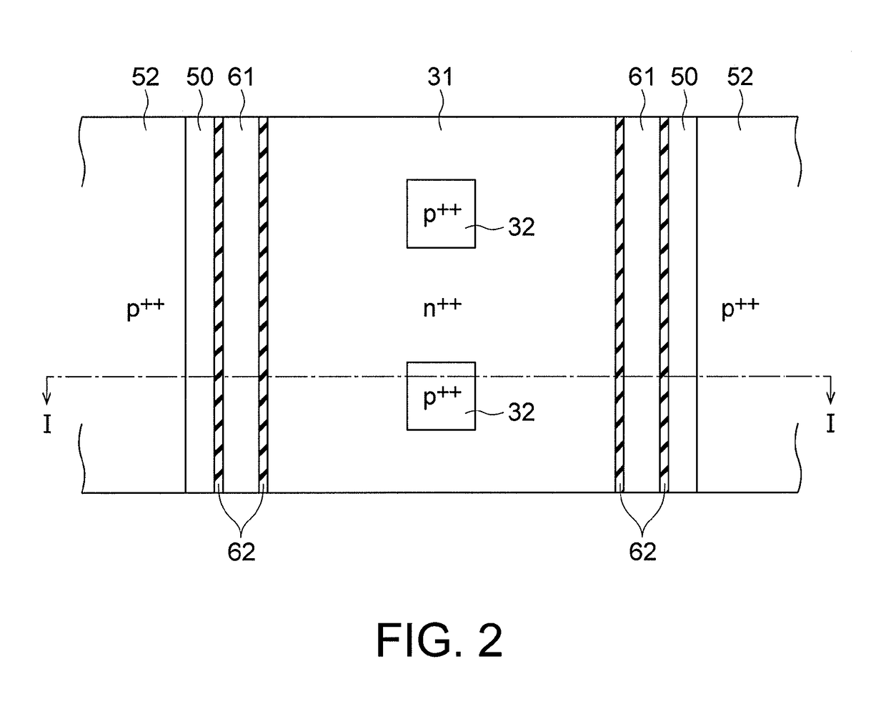
[0047]As shown in FIG. 1, the semiconductor device according to this embodiment includes an n-type semiconductor substrate 10 of high impurity concentration (the “n-type” corresponds to a “first conductivity type” in the claims), a n-type drift layer 20 of low impurity concentration formed on the n-type semiconductor substrate of high impurity concentration, a p-type base layer 30 disposed on the drift layer 20 (the “p-type” corresponds to a “second conductivity ...

second embodiment

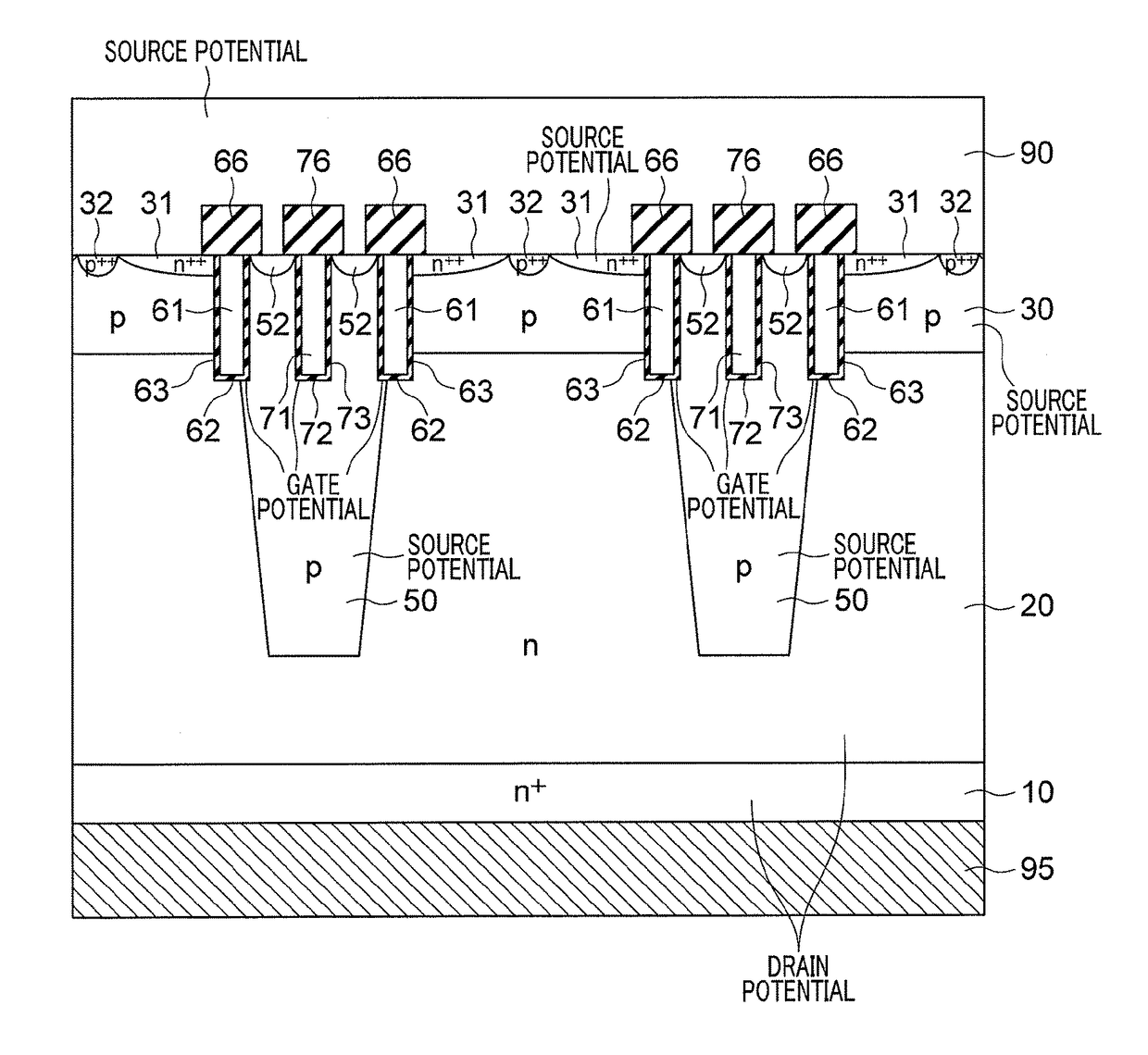
[0073]Next, a second embodiment of the present invention will be described mainly with reference to FIGS. 4, 5 and 11.

[0074]According to the second embodiment, in addition to the first gate electrode 61 and the first insulating layer 62 according to the first embodiment, a second gate electrode 71 surrounded by a second insulating layer 72 is provided in the column layer at an intermediate position in the horizontal direction between the pair of first gate electrodes 61. The second insulating layer 72 and the second gate electrode 71 are disposed in a second trench 73 formed in the column layer 50. The second gate electrode 71 is also at the gate potential.

[0075]In addition, according to this embodiment, a second interlayer insulating film 76 is formed on an upper surface of the second gate electrode 71 and the second insulating layer 72. Viewed from above, the second gate electrode 71, the second insulating layer 72 and the second interlayer insulating film 76 are shaped in a strip...

third embodiment

[0083]Next, a third embodiment of the present invention will be described mainly with reference to FIGS. 6 to 8.

[0084]According to the third embodiment, in addition to the first gate electrode 61 and the first insulating layer 62 according to the first embodiment, a third gate electrode 81 surrounded by a third insulating layer 82 is provided between two adjacent column layers 50. The third insulating layer 82 and the third gate electrode 81 are disposed in a third trench 83 that extends from the source region 31 into the drift layer 20. The third gate electrode 81 is also at the gate potential.

[0085]In addition, according to this embodiment, a third interlayer insulating film 86 is formed on an upper surface of the third gate electrode 81 and the third insulating layer 82. Viewed from above, the third gate electrode 81, the third insulating layer 82 and the third interlayer insulating film 86 are shaped in a striped pattern (see FIG. 7 for the third gate electrode 81 and the third ...


PUM


Abstract

A semiconductor device includes a drift layer 20 of a first conductivity type, a base layer 30 of a second conductivity type that is disposed on the drift layer 20 and is connected to a source electrode 90, and a column layer 50 of a second conductivity type that is connected to the source electrode 90 and penetrates the base layer 30 to extend into the drift layer 20.

Description

CROSS-REFERENCE TO RELATED APPLICATION(S)[0001]This application is the U.S. National Stage of International Patent Application No. PCT / JP2014 / 059515 filed on Mar. 31, 2014, the disclosure of which is incorporated in its entirety herein by reference.TECHNICAL FIELD[0002]The present invention relates to a semiconductor device.BACKGROUND ART[0003]A known conventional semiconductor device includes a semiconductor substrate of a first conductivity type, a pillar layer including a first semiconductor pillar sub-layer of the first conductivity type and a second semiconductor pillar sub-layer of a second conductivity type that is formed on the semiconductor substrate and has a rectangular strip-like shape in cross section, a first main electrode electrically connected to the semiconductor substrate, a semiconductor base layer of the second conductivity type formed on a surface of the first semiconductor pillar sub-layer, a second main electrode that is directly joined to a semiconductor dif...

Claims


Application Information

Patent Timeline
Patent Type & Authority Patents(United States)
IPC IPC(8): H01L29/768H01L29/08H01L29/06H01L29/78H01L29/10
CPCH01L29/7813H01L29/0634H01L29/0696H01L29/7811H01L29/1095H01L29/7802H01L29/0865H01L29/407H01L29/4238H01L29/66734
Inventor ASADA, TAKESHIKITADA, MIZUEYAMAGUCHI, TAKESHISUZUKI, NORIAKI
Owner SHINDENGEN ELECTRIC MFG CO LTD
Why Eureka
Try Eureka