Check patentability & draft patents in minutes with Patsnap Eureka AI!

Simulation method of FLASH/electrically erasable programmable read-only memory (EEPROM)

A simulation method and functional technology, applied in the field of smart card chip simulation, can solve problems such as difficult assembly and implementation, no FLASH/EEPROM implementation form, etc.

Inactive Publication Date: 2010-06-23
BEIJING CEC HUADA ELECTRONIC DESIGN CO LTD
View PDF0 Cites 3 Cited by
  • Summary
  • Abstract
  • Description
  • Claims
  • Application Information

AI Technical Summary

Problems solved by technology

[0003] 1. Usually, an emulator is required before the chip is implemented, and at this time there is no implementation form of FLASH/EEPROM, especially as an embedded FLASH/EEP

Method used


Image

  • Simulation method of FLASH/electrically erasable programmable read-only memory (EEPROM)
  • Simulation method of FLASH/electrically erasable programmable read-only memory (EEPROM)
  • Simulation method of FLASH/electrically erasable programmable read-only memory (EEPROM)

Examples


Example Embodiment

[0011] The present invention will be further described below in conjunction with the drawings.

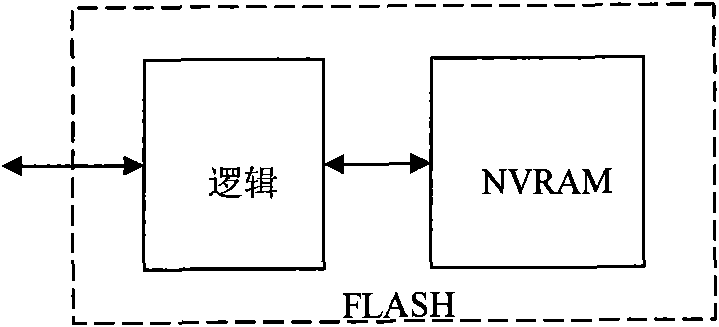
[0012] The invention discloses a FLASH / EEPROM simulation method based on NVRAM, which uses the characteristics of NVRAM to save data after power-off, and simulates the data storage function of FLASH / EEPROM; through logic circuits, it simulates FLASH / EEPROM erasing and programming Timing; Use FPGA internal RAM to simulate the page buffer area of ​​FLASH / EEPROM;

[0013] Use FPGA internal logic to realize the function of erasing "1" and writing "0" of FLASH / EEPROM.

[0014] The logic circuit is described as follows:

[0015] Design a counting logic, such as figure 2 As shown, whether it is an erasing operation or a programming operation, the address signal of the NVRAM is generated by the output signal of the counter and the external input address signal at the same time. The read and write signal is generated according to the counter when it reaches a certain time, combined with the progra...


PUM


Abstract

The invention provides a simulation method of FLASH/electrically erasable programmable read-only memory (EEPROM), which is based on a logical add non-volatile random access memory (NVRAM) combination and belongs to the technical field of intelligent card simulation. A structure and a time sequence based on the FLASH/EEPROM are realized by adopting a logic mode, a mode of a counter is adopted in the logic to realize the time sequence of the FLASH/EEPROM, and various logic signals are realized on the basis of realizing the time sequence of the FLASH/EEPROM.

Description

technical field [0001] The invention relates to the technical field of smart card chip emulation. Background technique [0002] In the smart card chip emulator, the emulation of the FLASH / EEPROM module will be involved, [0003] 1. Usually, an emulator is required before chip implementation, but at this time there is no implementation form of FLASH / EEPROM, especially as an embedded FLASH / EEPROM module. [0004] 2. Considering the compatibility of the emulator, FLASH / EEPROM has various packaging forms and pin arrangements, and it is not easy to assemble on the same PCB. [0005] A method of simulating FLASH / EEPROM by using NVRAM plus logic circuit proposed by the present invention can solve such problems. Contents of the invention [0006] The present invention adopts the function of NVRAM power-off data not being lost, simulates the data non-volatile characteristics of FLASH / EEPROM; adopts the combination of FPGA logic and NVRAM to realize the simulation of FLASH / EEPROM,...

Claims


Application Information

Patent Timeline
IPC IPC(8): G06F11/36
Inventor 李丹
Owner BEIJING CEC HUADA ELECTRONIC DESIGN CO LTD
Features
  • R&D
  • Intellectual Property
  • Life Sciences
  • Materials
  • Tech Scout
  • Unparalleled Data Quality
  • Higher Quality Content
  • 60% Fewer Hallucinations
Learn More