
Liquid crystal display panel

A liquid crystal display panel and substrate technology, applied in nonlinear optics, instruments, optics, etc., can solve problems such as image sticking, affecting image quality, and unclear dumping direction, and achieve the effect of reducing image sticking

Active Publication Date: 2011-07-27
AU OPTRONICS CORP
View PDF0 Cites 0 Cited by
  • Summary
  • Abstract
  • Description
  • Claims
  • Application Information

AI Technical Summary

Problems solved by technology

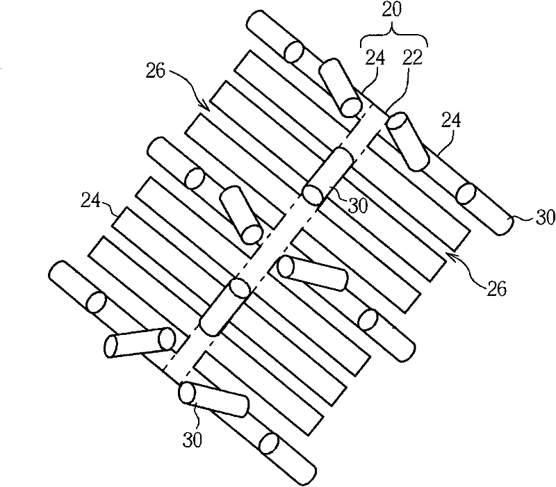
Although the liquid crystal molecules 30 corresponding to the fine slits 26 can have a clear directionality of tilting, the liquid crystal molecules corresponding to the main electrode strips have an unclear direction of tilting.
Therefore, many nodes will randomly appear in the backbone part of the pixel, and random nodes will easily cause image retention (IR) when displaying the picture, thus affecting the image quality

Method used


Image

  • Liquid crystal display panel
  • Liquid crystal display panel
  • Liquid crystal display panel

Examples


Embodiment Construction

[0039] The following are detailed descriptions and accompanying drawings of the present invention. However, the accompanying drawings are only for reference and auxiliary description, and are not intended to limit the present invention.

[0040] In order to enable those skilled in the art to which the present invention belongs to have a better understanding of the present invention, a number of preferred embodiments of the present invention are enumerated below, together with the accompanying drawings, to describe in detail the composition of the present invention and the desired effects .

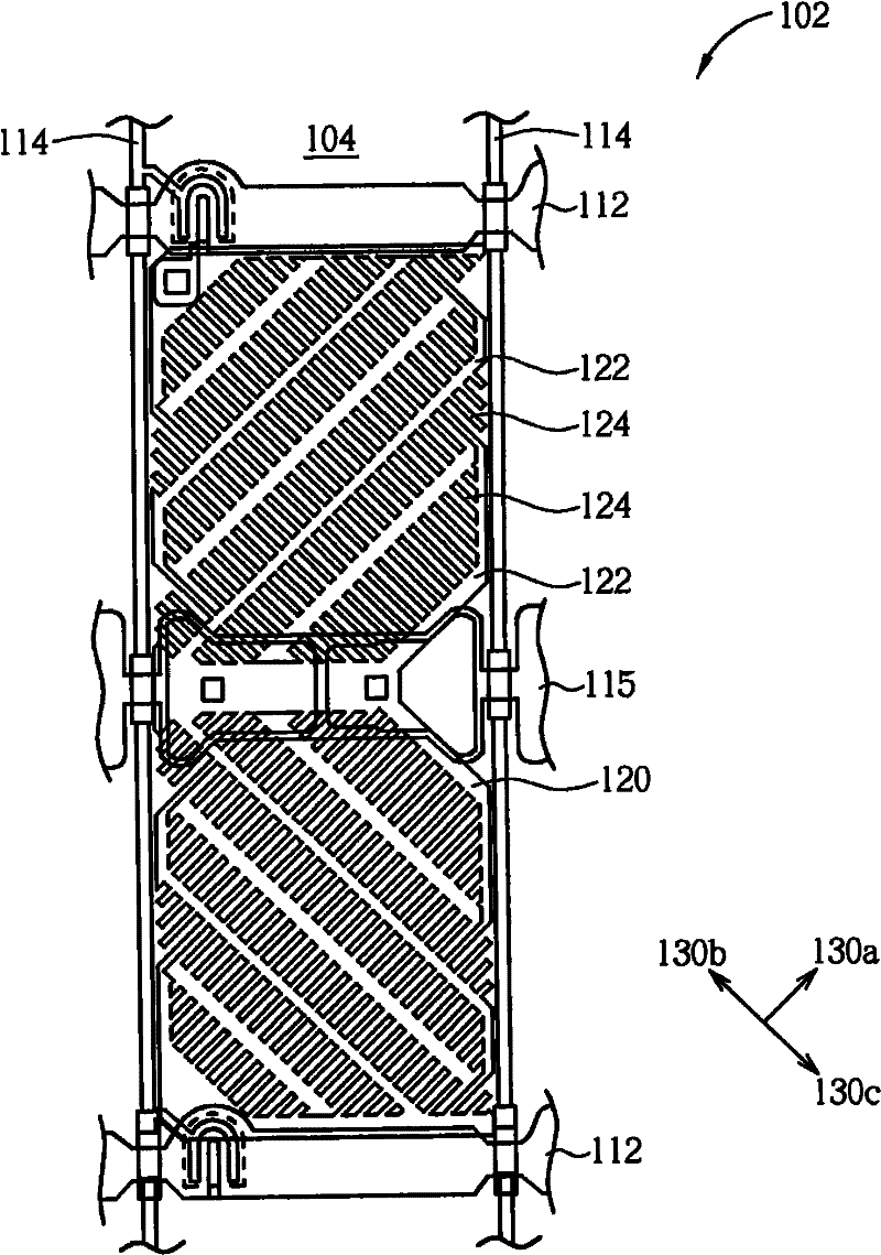
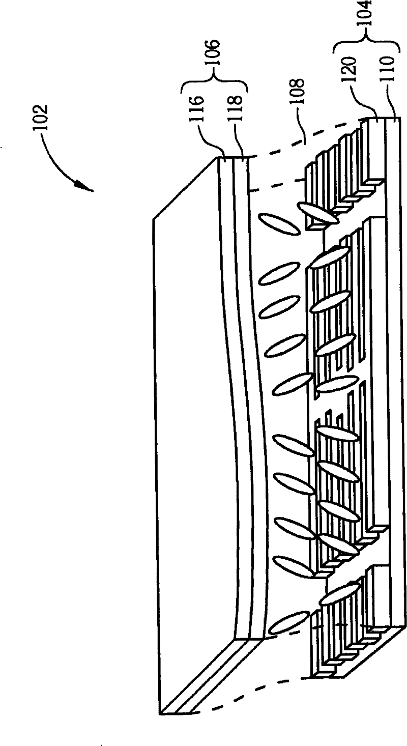
[0041] Please refer to Figure 2 to Figure 4 . Figure 2 to Figure 4 It is a schematic diagram of a preferred embodiment of the sub-pixel structure of the liquid crystal display panel of the present invention, for example, one of the red-green-blue (RGB) sub-pixel structures. figure 2 is the top view of the sub-pixel structure, image 3 is a three-dimensional cross-sectional schematic...


PUM


Abstract

The invention discloses a liquid crystal display panel. The liquid crystal display panel comprises a first substrate, a second substrate, a plurality of first secondary electrode branches, a plurality of second secondary electrode branches and a liquid crystal layer, wherein the first substrate comprises a common electrode; the second substrate comprises at least one pixel electrode which comprises at least one main electrode strip, both sides of the main electrode strip are provided with a first edge and a second edge which are opposite to each other, and the main electrode strip extends to a first direction; the plurality of first secondary electrode branches extend outwards from the first edge of the main electrode strip; the plurality of second secondary electrode branches extend outwards from the second edge of the main electrode strip, each first secondary electrode branch and each second secondary electrode branch have a branch width, each second secondary electrode branch has a position offset from the first direction relative to each first secondary electrode branch, and the position offset is more than zero and less than the branch width of each first secondary electrodebranch and each second secondary electrode branch; and the liquid crystal layer is arranged between the first substrate and the second substrate.

Description

[0001] This patent application is a divisional application of the Chinese patent application with the application number 200910001601.3 and the invention name "liquid crystal display panel" submitted on January 05, 2009. technical field [0002] The present invention relates to a liquid crystal display panel, in particular to a fine-slit stabilized multi-domain vertical alignment (FSMVA for short) liquid crystal display panel. Background technique [0003] With the introduction of large-size liquid crystal display panels, the liquid crystal display panels must have wide viewing angles to meet the needs of use. Therefore, multi-domain vertical alignment (MVA) liquid crystal display panels with wide viewing angle characteristics have become mainstream products of large-size flat display panels. [0004] It is known that an array substrate (array substrate) of a multi-region vertically aligned liquid crystal display panel has patterned pixel electrodes, and a color filter subst...

Claims


Application Information

Patent Timeline
Patent Type & Authority Patents(China)
IPC IPC(8): G02F1/1343G02F1/139
Inventor 吕婉华李佳育廖培钧张庭瑞
Owner AU OPTRONICS CORP
Learn More