
Liquid crystal display device and method for fabricating the same

a technology of liquid crystal display and liquid crystal, which is applied in the direction of instruments, non-linear optics, optics, etc., can solve the problems of light leakage or other problems, image quality deterioration, and light leakage in these regions, so as to prevent light leakage, reduce fabrication costs, and prevent the effect of reducing the transmittan

Inactive Publication Date: 2006-07-06
LG DISPLAY CO LTD
View PDF20 Cites 37 Cited by
  • Summary
  • Abstract
  • Description
  • Claims
  • Application Information

AI Technical Summary

Benefits of technology

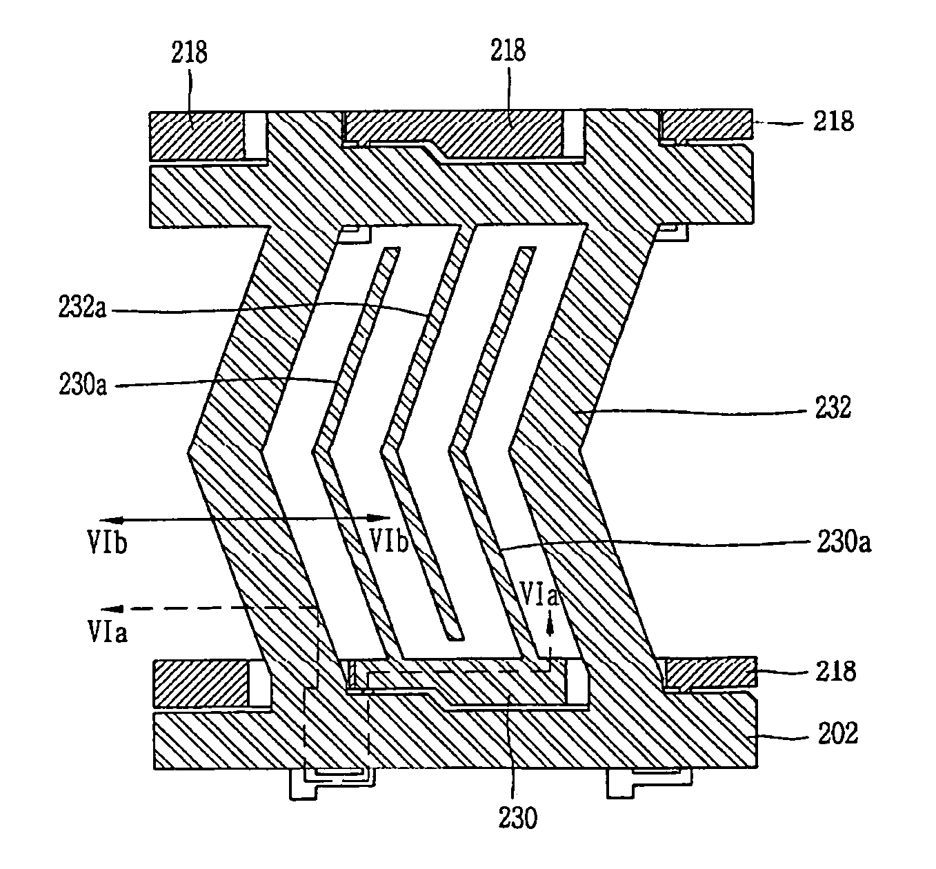
The present invention is about a liquid crystal display device with a color filter on thin film transistor structure and a method for fabricating it. The technical effects of this invention include preventing leakage of light caused by a disclination in a COT structure, reducing fabrication cost, and preventing decrease in transmittance. The invention provides an array substrate of a liquid crystal display device with common electrode parts arranged at both sides of the data line to shield the data line, a thin film transistor formed at an crossing of the gate line and the data line, a black matrix over a region including the data lines and a portion of the common electrode parts, and a color filter arranged at the pixel region. The invention also provides a liquid crystal display device with a plurality of gate lines and a plurality of data lines crossing each other to define a pixel region on a substrate, a plurality of common electrode lines, a pair of common electrode parts corresponding to each one of the data lines, a black matrix over a region including the data lines and a portion of the common electrode parts, and a color filter arranged at the pixel region.

Problems solved by technology

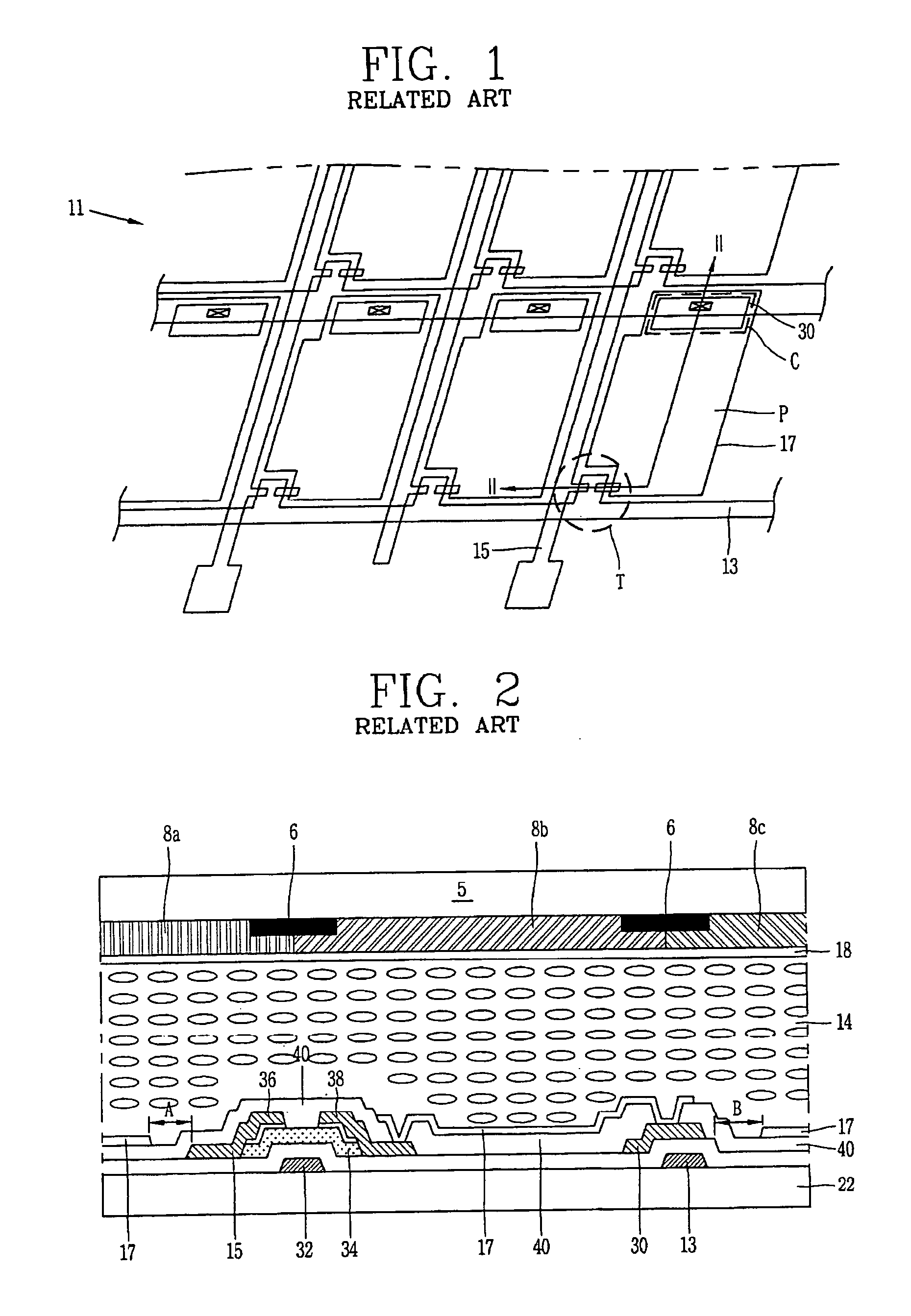
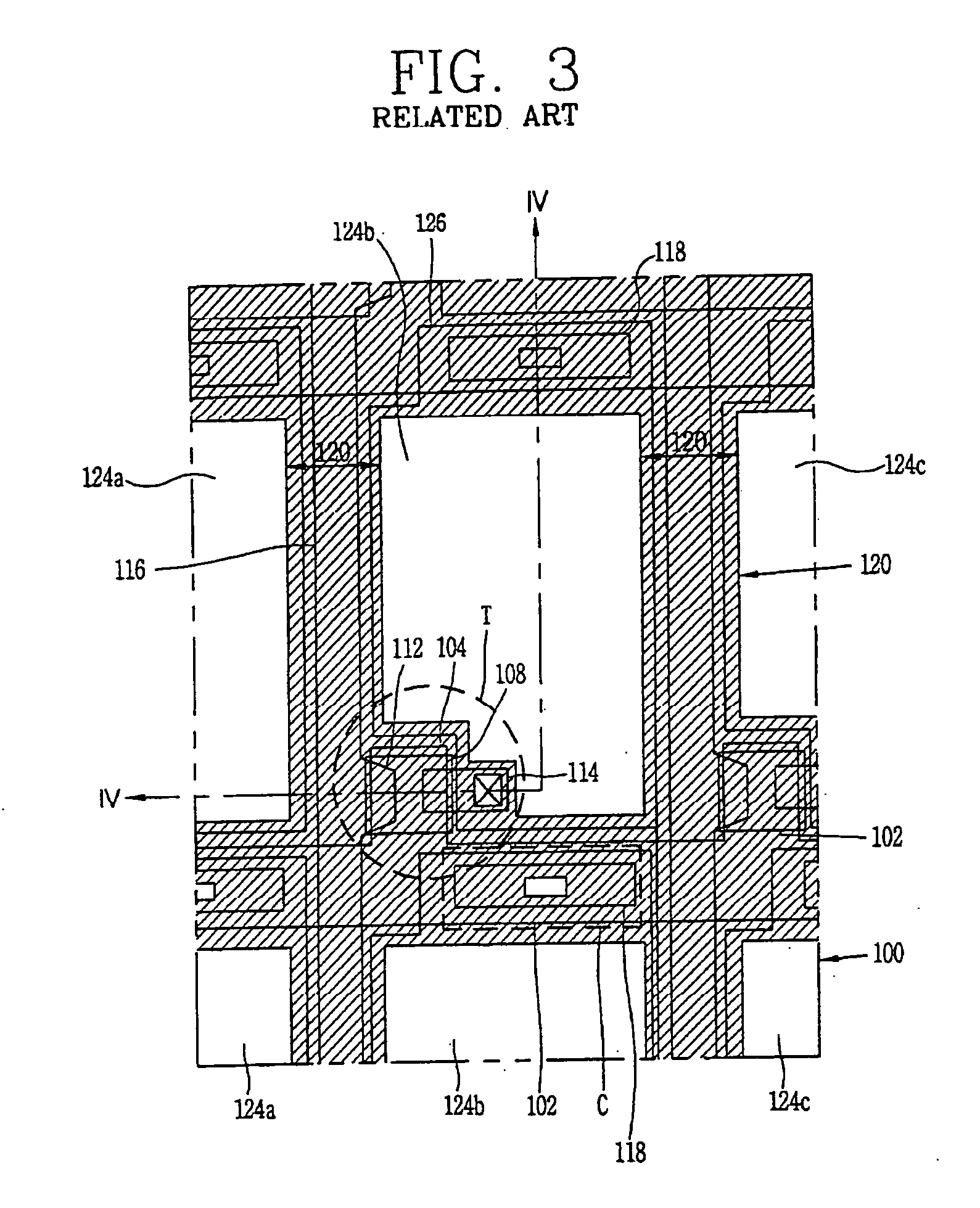
As described above, when the liquid crystal panel is formed by attaching the upper color filter substrate (not shown) and the lower array substrate (not shown), light leakage or other problems may occur because of misalignment between the color filter substrate (not shown) and the array substrate (not shown).
Thus, light leakage occurs in these regions.
Accordingly, image quality deteriorates.
However, the use of the acryl material increases cost.

Method used


Image

  • Liquid crystal display device and method for fabricating the same
  • Liquid crystal display device and method for fabricating the same
  • Liquid crystal display device and method for fabricating the same

Examples


Embodiment Construction

[0044] Reference will now be made in detail to the preferred embodiments of the present invention, examples of which are illustrated in the accompanying drawings.

[0045]FIGS. 5A to 5D are plane views sequentially showing the layout of a liquid crystal display having a COT structure in accordance with an embodiment of the present invention. Referring to FIG. 5A, a gate line 202 is arranged horizontally on an array substrate. A common electrode line 206 is horizontally arranged at a specific interval from the gate line 202. The common electrode line 206 includes a data line shielding common electrode part 206a vertically arranged to minimize the cross-talk level, and a storage capacitor part 206b horizontally arranged to form a storage capacitor. In one embodiment of the present invention, at least two data line shielding common electrode parts 206a are arranged to face each other at a certain interval therebetween. Also, the gate line 202 and the common electrode line 206 are simulta...


PUM

PropertyMeasurementUnit
thicknessaaaaaaaaaa
optical anisotropyaaaaaaaaaa
double refraction propertiesaaaaaaaaaa

Abstract

A liquid crystal display device includes a gate line and a data line crossing each other to define a pixel region on a substrate; common electrode parts arranged at both sides of the data line to shield the data line; a black matrix over a region including the data line and a portion of the common electrode parts; and a color filter arranged at the pixel region.

Description

[0001] This application claims the benefit of Korean Patent Application Nos. 2004-118478 and 2005-46945 filed in Korea on Dec. 31, 2004, and Jun. 1, 2005, respectively, both of which are hereby incorporated by reference in their entirety. BACKGROUND OF THE INVENTION [0002] 1. Field of the Invention [0003] The present invention relates to a liquid crystal display device, and more particularly, to a liquid crystal display device having a color filter on thin film transistor structure and a method for fabricating the same. [0004] 2. Description of the Related Art [0005] In general, a liquid crystal display device (LCD) displays images using the optical anisotropy and double refraction properties of liquid crystal molecules. The arrangement of the liquid crystal molecules is changed by an applied electric field. The light transmittance of the liquid crystal molecules also changes in accordance with the alignment direction of the liquid crystal molecules. [0006] The LCD device includes t...

Claims


Application Information

Patent Timeline
Patent Type & Authority Applications(United States)
IPC IPC(8): G02F1/1343G02F1/1362
CPCG02F1/134363G02F1/136209G02F1/136213G02F1/136286G02F2001/136222G02F1/136222G02F1/1362
Inventor KIM, DONG-GUK
Owner LG DISPLAY CO LTD
Learn More