Liquid crystal display device

a technology of liquid crystal display and display device, which is applied in the direction of semiconductor devices, instruments, metallic oxides, etc., can solve the problems of image quality degradation, and achieve the effect of stabilizing the operation characteristics of thin film transistors

Active Publication Date: 2010-06-03
SEMICON ENERGY LAB CO LTD
View PDF101 Cites 37 Cited by
  • Summary
  • Abstract
  • Description
  • Claims
  • Application Information

AI Technical Summary

Benefits of technology

[0025]In a liquid crystal display device which includes a thin film transistor formed by using an oxide semiconductor layer for a channel, an interlayer film which covers at least the oxide semiconductor layer i

Problems solved by technology

In the case of providing a color filter layer on the counter substrate side, precise positional alignment of a pixel region with an elemen

Method used


Image

  • Liquid crystal display device
  • Liquid crystal display device
  • Liquid crystal display device

Examples


embodiment 1

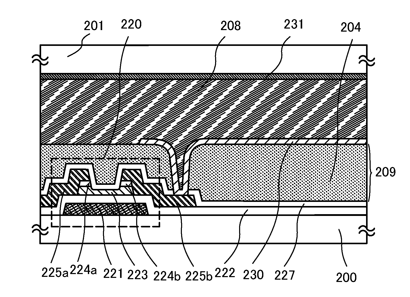
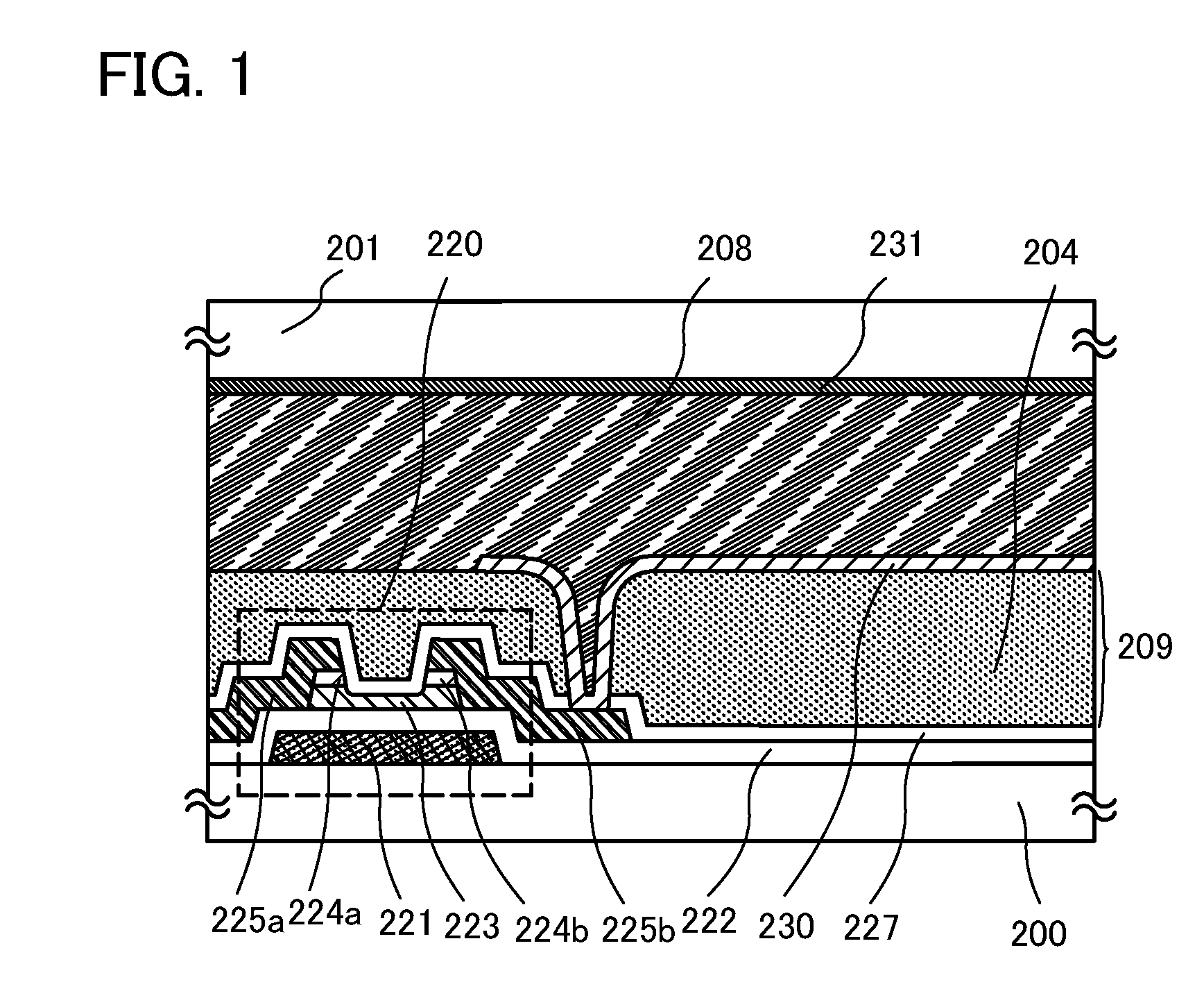
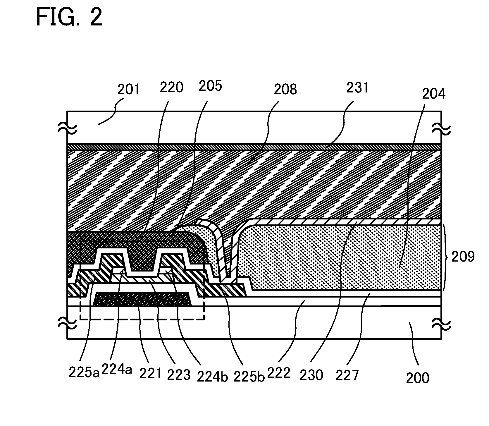
[0047]Liquid crystal display devices and manufacturing methods thereof will be described with reference to FIG. 1, FIG. 2, and FIGS. 17A and 17B.

[0048]FIG. 1, FIG. 2, and FIGS. 17A and 17B are cross-sectional views of liquid crystal display devices.

[0049]In FIG. 1 and FIG. 2, an element layer 203 (see FIGS. 17A and 17B) is formed over a first substrate 200 which is an element substrate, an interlayer film 209 is formed over the element layer 203, and a pixel electrode layer 230 is provided over the interlayer film 209. A liquid crystal layer 208 is sealed between the pixel electrode layer 230 and a counter electrode layer 231 formed on a second substrate 201 which is a counter substrate.

[0050]A mode of a liquid crystal display device illustrated in FIG. 1 includes a plurality of pixels in matrix. In each of the pixels, a thin film transistor including an oxide semiconductor layer, an interlayer film over the thin film transistor, a pixel electrode layer over the interlayer film, and...

embodiment 2

[0079]A liquid crystal display device will be described with reference to FIGS. 18A and 18B.

[0080]FIG. 18A is a plan view of a liquid crystal display device illustrating one pixel.

[0081]FIG. 18B is a cross-sectional view taken along line X1-X2 in FIG. 18A.

[0082]In FIG. 18A, a plurality of source wiring layers (including a wiring layer 405a) are provided in parallel to each other (extended in a vertical direction in the drawing) and apart from each other. A plurality of gate wiring layers (including a gate electrode layer 401) are provided apart from each other and extend in a direction generally perpendicular to the source wiring layers (a horizontal direction in the drawing). Common wiring layers 408 are provided adjacent to the plurality of gate wiring layers and extend in a direction generally parallel to the gate wiring layers, that is, in a direction generally perpendicular to the source wiring layers (a horizontal direction in the drawing). Roughly rectangular spaces are surro...

embodiment 3

[0131]In Embodiment 3, examples in which a pixel electrode layer and a common electrode layer are formed in different planes will be described with reference to FIGS. 3A and 3B, FIGS. 4A and 4B, and FIGS. 7A and 7B. Note that components in common with those in Embodiments 1 and 2 can be formed using a similar material and manufacturing method, and detailed description of the same portions and portions having similar functions is omitted.

[0132]FIG. 3A, FIG. 4A, and FIG. 7A are plan views of liquid crystal display devices, each illustrating one pixel. FIG. 3B, FIG. 4B, and FIG. 7B are cross-sectional views taken along line X1-X2 in FIG. 3A, FIG. 4A, and FIG. 7A, respectively.

[0133]In each of the plan views of FIG. 3A, FIG. 4A, and FIG. 7A, in a manner similar to that of Embodiment 2, a plurality of source wiring layers (including a wiring layer 405a) are provided in parallel to each other (extended in a vertical direction in the drawing) and apart from each other. A plurality of gate ...


PUM


Abstract

To provide a liquid crystal display device suitable for a thin film transistor which uses an oxide semiconductor. In a liquid crystal display device which includes a thin film transistor including an oxide semiconductor layer, a film having a function of attenuating the intensity of transmitting visible light is used as an interlayer film which covers at least the oxide semiconductor layer. As the film having a function of attenuating the intensity of transmitting visible light, a coloring layer can be used and a light-transmitting chromatic color resin layer is preferably used. An interlayer film which includes a light-transmitting chromatic color resin layer and a light-blocking layer may be formed in order that the light-blocking layer is used as a film having a function of attenuating the intensity of transmitting visible light.

Description

BACKGROUND OF THE INVENTION[0001]1. Field of the Invention[0002]The present invention relates to a liquid crystal display device in which an oxide semiconductor is used and a manufacturing method thereof.[0003]2. Description of the Related Art[0004]As typically seen in a liquid crystal display device, a thin film transistor formed over a flat plate such as a glass substrate is manufactured using amorphous silicon or polycrystalline silicon. A thin film transistor manufactured using amorphous silicon has low field effect mobility, but can be formed over a large glass substrate. In contrast, a thin film transistor manufactured using crystalline silicon has high field effect mobility, but due to a crystallization step such as laser annealing, such a transistor is not always suitable for being formed over a large glass substrate.[0005]In view of the foregoing, attention has been drawn to a technique by which a thin film transistor is manufactured using an oxide semiconductor and such a ...

Claims


Application Information

Patent Timeline
IPC IPC(8): G09G3/36
CPCG02F1/133514G02F1/136209G02F2001/136222H01L27/1248G02F1/1368H01L29/7869H01L27/1225G02F1/136222H01B3/10H01L29/78618
Inventor ISHITANI, TETSUJIKUBOTA, DAISUKE
Owner SEMICON ENERGY LAB CO LTD
Why Eureka
Try Eureka