
Integrated electronic device and method of making the same

a technology of integrated electronic devices and integrated circuits, which is applied in the direction of transformers/inductance coils/windings/connections, multi-port networks, basic electric elements, etc., can solve the problems of preventing the application of a targeted high, ltcc-produced ipds showing insufficient q factor in many cases, and reducing the size of integrated electronic devices

Active Publication Date: 2007-03-01
TAIYO YUDEN KK
View PDF5 Cites 115 Cited by
  • Summary
  • Abstract
  • Description
  • Claims
  • Application Information

AI Technical Summary

Benefits of technology

[0016] Further, according to the multi-stage coil inductor in the present integrated electronic device, the applied AC current flows in the same direction in the mutually adjacent spiral coils, whereby intensity of the magnetic field generated between the coils is reduced to decrease skin effect of the high frequency current in the coil wires. Therefore, it is possible to lower the resistance Ri (high frequency resistance) of the coil wire. As understood from Formula (1), lowering of the resistance Ri contributes to an increase in the Q factor.
[0033] Preferably, the substrate has a recess, and the multi-stage coil inductor is provided in the recess. Such an arrangement is suitable for reducing the size of the integrated electronic device.

Problems solved by technology

Accordingly, IPDs manufactured by LTCC do not show a sufficient Q factor in many cases.
Thus, due to the insufficient Q factor, IPDs manufactured by LTCC technology are sometimes prevented from applying to a targeted high-frequency band and achieving a favorable high-frequency characteristic.

Method used


Image

  • Integrated electronic device and method of making the same
  • Integrated electronic device and method of making the same
  • Integrated electronic device and method of making the same

Examples


Embodiment Construction

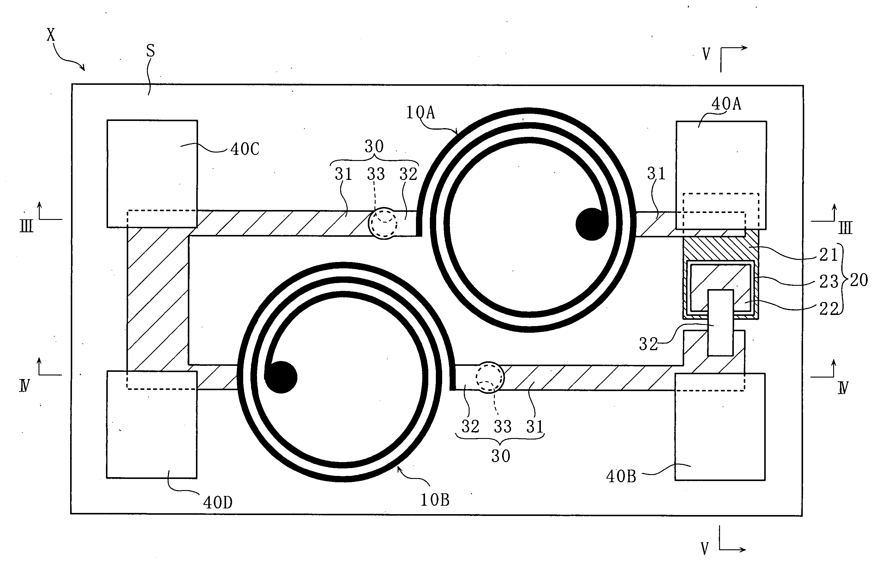
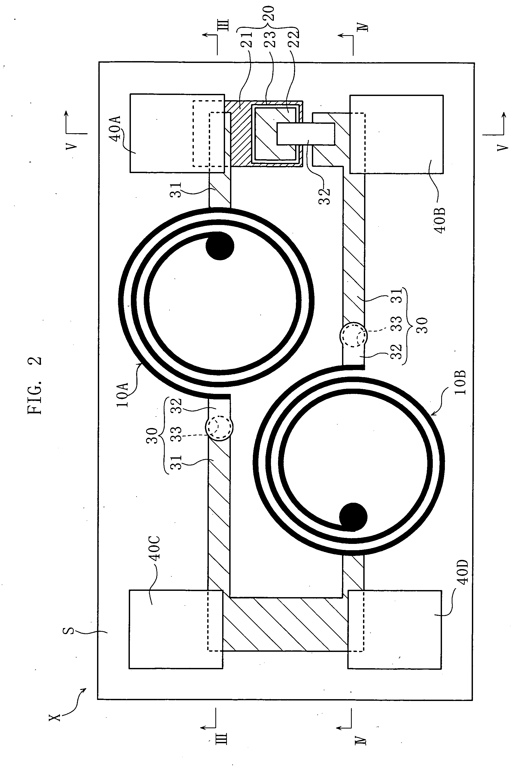
[0070]FIG. 2 through FIG. 5 show an integrated electronic device X according to the present invention. FIG. 2 is a plan view of the integrated electronic device X. FIG. 3 through FIG. 5 are sectional views taken in lines III-III, IV-IV, and V-V in FIG. 2 respectively.

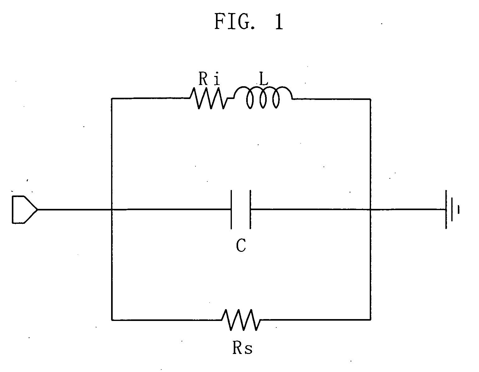
[0071] The integrated electronic device X includes a substrate S, multi-stage coil inductors 10A, 10B, a capacitor 20, three-dimensional wiring 30, and pads 40A, 40B, 40C, 40D, constituting a circuit shown in FIG. 6.

[0072] The substrate S is provided by a semiconductor substrate, a semiconductor substrate having a surface formed with an insulation film, a quartz substrate, a glass substrate, a piezoelectric substrate, a ceramic substrate, an SOI (silicon on insulator) substrate, a SOQ (silicon on quartz) substrate or an SOG (silicon on glass) substrate. The semiconductor substrate is made up of a silicon material such as monocrystal silicon. The piezoelectric substrate is made up of piezoelectric materials such as LiT...


PUM


Abstract

An integrated electronic device includes a substrate, passive components, pads for external connection, and three-dimensional wiring. The passive components includes a multi-stage coil inductor provided on the substrate. The multi-stage coil inductor has a plurality of coils disposed in several layers. Mutually adjacent coil wires are spaced-apart from each other. The three-dimensional wiring includes a first wiring portion which extends on the substrate, a second wiring portion which extends off the substrate but along the substrate, and a third wiring portion connecting with the first wiring portion and the second wiring portion.

Description

BACKGROUND OF THE INVENTION [0001] 1. Field of the Invention [0002] The present invention relates to an integrated electronic device provided with a plurality of passive components such as inductors. The present invention also relates to a method of manufacturing such an integrated electronic device. [0003] 2. Description of the Related Art [0004] An RF (radio frequency) system or RF circuitry incorporated in e.g. a mobile terminal generally includes an IPD (integrated passive device) functioning as high-frequency module devices in order to achieve high performance, small size, light weight, etc. An IPD incorporates passive components such as inductors, capacitors, resistors and filters. Among these components, inductors tend to have a lower Q factor (quality factor) than e.g. capacitors. When an IPD includes an inductor, the entire IPD is also likely to have a low Q factor. Therefore, there are demands for IPDs with high Q factor. Further, since RF systems have utilized higher freq...

Claims


Application Information

Patent Timeline
IPC IPC(8): H01L29/00H01L23/52H01F27/28H01F5/00
CPCH01F17/0006H01L23/5227H01L27/0688H01L2924/09701H01L2924/0002H01L2924/3011H01L2924/00H03H7/38
Inventor MI, XIAOYUMIZUNO, YOSHIHIROMATSUMOTO, TSUYOSHIOKUDA, HISAOUEDA, SATOSHI
Owner TAIYO YUDEN KK
Learn More