Double-sided touch-sensitive panel with shield and drive combined layer

a combined layer and touch-sensitive panel technology, applied in the field of capacitive multi-touch sensor panels, can solve the problems of noise appearing on the columns, and achieve the effect of preventing the capacitive coupling of a modulated vcom layer, and saving spa

Active Publication Date: 2011-04-05
APPLE INC
View PDF28 Cites 692 Cited by
  • Summary
  • Abstract
  • Description
  • Claims
  • Application Information

AI Technical Summary

Benefits of technology

[0008]A multi-touch sensor panel can be created using a substrate with column and row traces formed on either side of the substrate using a novel fabrication process. Flex circuits can be used to connect the column and row traces on either side of the sensor panel to its associated sensor panel circuitry. Traces made of copper or other highly conductive metals running along the edge of the substrate can be used to bring the row traces to the same edge of the substrate as the column traces so that the flex circuits can be bonded to the same edge of the substrate on directly opposing sides of the substrate, minimizing the area needed for connectivity and reducing the overall size of the sensor panel. A single flex circuit can be fabricated to connect to the rows and columns on directly opposing sides at the same edge of the substrate. Furthermore, the row traces can be widened to shield the column traces from a modulated Vcom layer.
[0011]Flex circuit portions on a single flex circuit can be formed for connecting to the row and column traces, respectively, on either side of a DITO substrate, and to a host processor. The flex circuit can also include a circuit area upon which a multi-touch subsystem, multi-touch panel processor, high voltage driver and decoder circuitry, an EEPROM and some essential small components such as bypass capacitors can be mounted and connected to save space.
[0012]The rows of the DITO substrate can also be widened for shielding purposes and for providing a uniform appearance according to embodiments of this invention. To prevent the capacitive coupling of a modulated Vcom layer onto the columns of the substrate, the rows may be widened. The number of rows does not change, but they can be much wider, leaving only about 30 microns of space between them. Because these wider rows are not isolated but are instead either held at a DC voltage or stimulated with a stimulation voltage, these wider rows act as a shield, preventing a modulated Vcom layer from capacitively coupling onto the columns. In addition, because of the narrow spacing between them, the wide rows provide a uniform appearance. Thus, shielding, modulation and a uniform appearance can be obtained from a single layer of ITO.

Problems solved by technology

Furthermore, when a transparent capacitive touch sensor panel is bonded to a liquid crystal display (LCD), a modulated Vcom layer in the LCD can couple onto the columns of the sensor panel, causing noise to appear on the columns.

Method used


Image

  • Double-sided touch-sensitive panel with shield and drive combined layer
  • Double-sided touch-sensitive panel with shield and drive combined layer
  • Double-sided touch-sensitive panel with shield and drive combined layer

Examples


Embodiment Construction

[0026]In the following description of preferred embodiments, reference is made to the accompanying drawings which form a part hereof, and in which it is shown by way of illustration specific embodiments in which the invention may be practiced. It is to be understood that other embodiments may be utilized and structural changes may be made without departing from the scope of the preferred embodiments of the present invention.

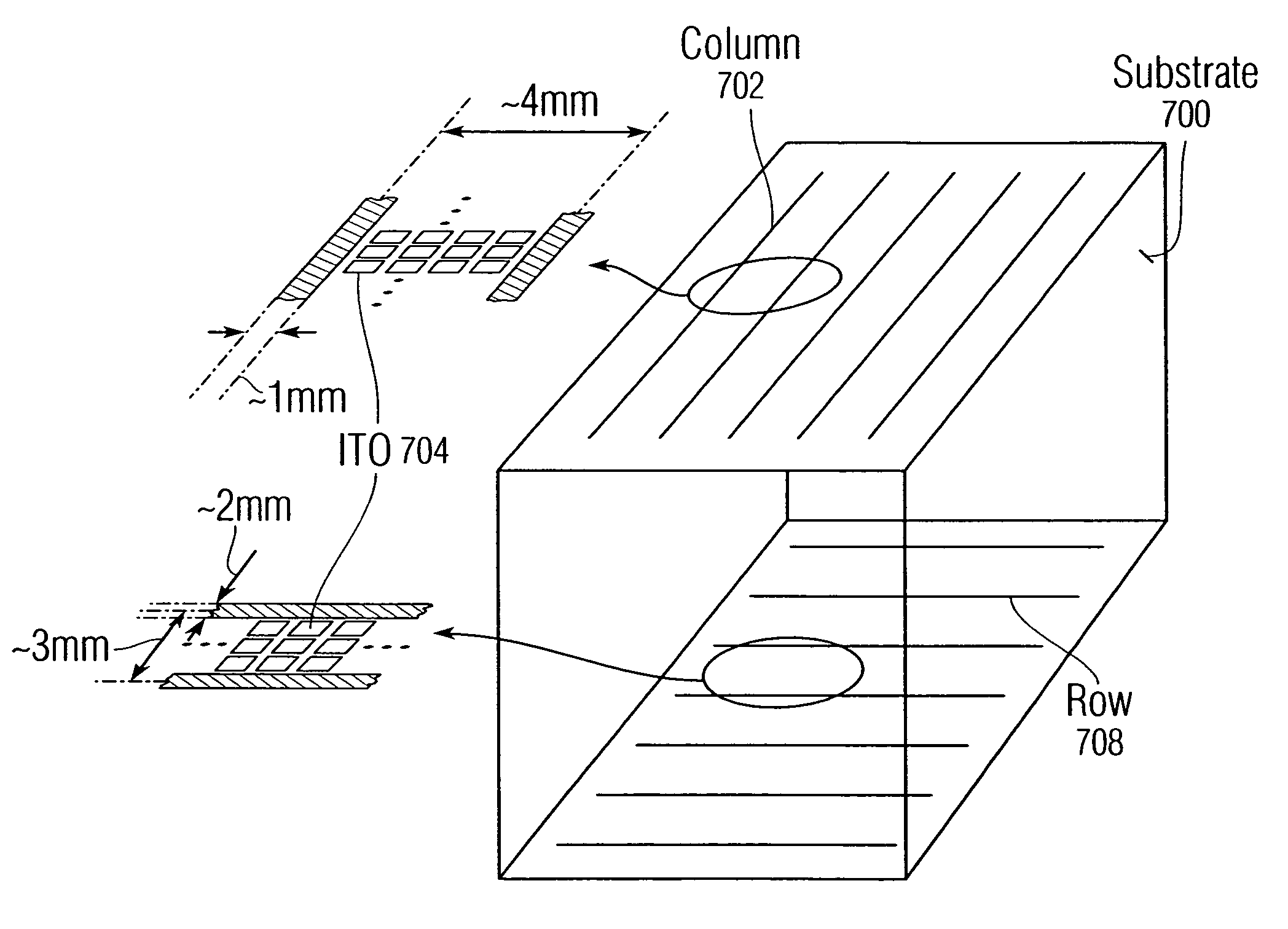
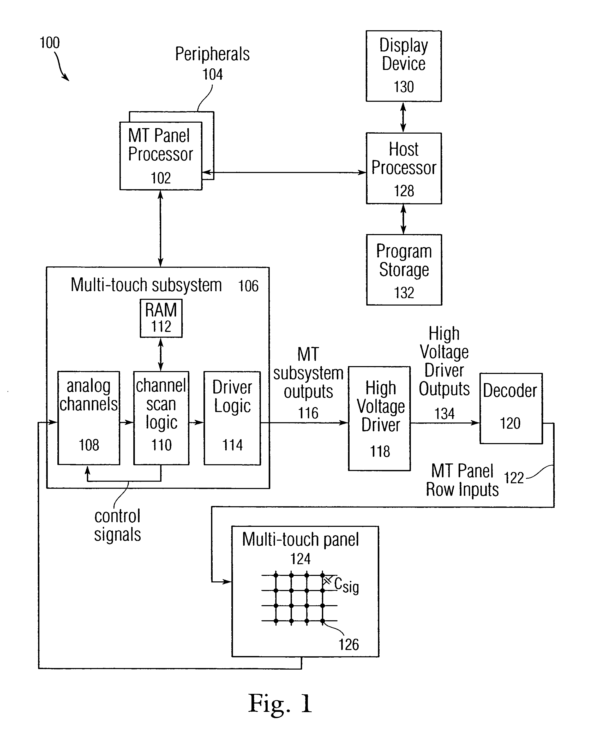
[0027]Multi-touch sensor panels and their associated sensor panel circuitry may be able to detect multiple touches (touch events or contact points) that occur at about the same time, and identify and track their locations. FIG. 1 illustrates exemplary computing system 100 operable with capacitive multi-touch sensor panel 124 according to embodiments of this invention. Multi-touch sensor panel 124 can be created using a substrate with column and row traces formed on either side of the substrate using a novel fabrication process. Flex circuits can be used to connec...


PUM


Abstract

A multi-touch capacitive touch sensor panel can be created using a substrate with column and row traces formed on either side of the substrate. To shield the column (sense) traces from the effects of capacitive coupling from a modulated Vcom layer in an adjacent liquid crystal display (LCD) or any source of capacitive coupling, the row traces can be widened to shield the column traces, and the row traces can be placed closer to the LCD. In particular, the rows can be widened so that there is spacing of about 30 microns between adjacent row traces. In this manner, the row traces can serve the dual functions of driving the touch sensor panel, and also the function of shielding the more sensitive column (sense) traces from the effects of capacitive coupling.

Description

FIELD OF THE INVENTION[0001]This invention relates to touch sensor panels, and more particularly, to capacitive multi-touch sensor panels having rows and columns formed on either sides of the same substrate.BACKGROUND OF THE INVENTION[0002]Many types of input devices are presently available for performing operations in a computing system, such as buttons or keys, mice, trackballs, touch panels, joysticks, touch screens and the like. Touch screens, in particular, are becoming increasingly popular because of their ease and versatility of operation as well as their declining price. Touch screens can include a touch panel, which can be a clear panel with a touch-sensitive surface. The touch panel can be positioned in front of a display screen so that the touch-sensitive surface covers the viewable area of the display screen. Touch screens can allow a user to make selections and move a cursor by simply touching the display screen via a finger or stylus. In general, the touch screen can r...

Claims


Application Information

Patent Timeline
Patent Type & Authority Patents(United States)
IPC IPC(8): G09G5/00
CPCG06F3/0416G06F3/044G06F1/1692G06F2203/04104G06F2203/04107G06F3/04164G06F3/04166G06F3/0445G06F3/0446G02F1/13338G06F3/0412G06F3/047G06F2203/04103G09G5/003G09G2300/04G02F1/133342
Inventor HOTELLING, STEVE PORTERLAND, BRIAN RICHARDS
Owner APPLE INC
Why Eureka
Try Eureka