High-density three-dimensional memory cell

a memory cell, high-density technology, applied in the direction of instruments, transistors, radio-controlled devices, etc., can solve the problems of increasing density, increasing the cost of substrates, and continual efforts to fabricate more circuitry, so as to reduce the feature size and height of portions of memory cells, the effect of improving density

Inactive Publication Date: 2005-10-04
SANDISK TECH LLC
View PDF7 Cites 698 Cited by
  • Summary
  • Abstract
  • Description
  • Claims
  • Application Information

AI Technical Summary

Benefits of technology

[0008]Other embodiments provide for improved density and decreased feature size and height of portions of the memory cell. For example, a preferred embodiment provides for a monolithic three dimensional memory array having an area density greater than about 5.0×10⁷ cells / mm2, while another calls for a three dimensional memory cell comprising a semiconductor element over a first conductor, wherein the cell has a feature size less than 2500 angstroms. Yet another provides for a monolithic three dimensional memory array having a cubic density greater than about 2.4×10¹⁰ cells / mm3. An additional embodiment provides for a three dimensional memory cell comprising a first conductor and a first semiconductor element over the first conductor, wherein the height of the first semiconductor element before planarizing is 4100 angstroms or less.

Problems solved by technology

This substrate is expensive, leading to continual efforts to fabricate more circuitry within a given area of substrate, increasing density.

Method used


Image

  • High-density three-dimensional memory cell
  • High-density three-dimensional memory cell
  • High-density three-dimensional memory cell

Examples


example

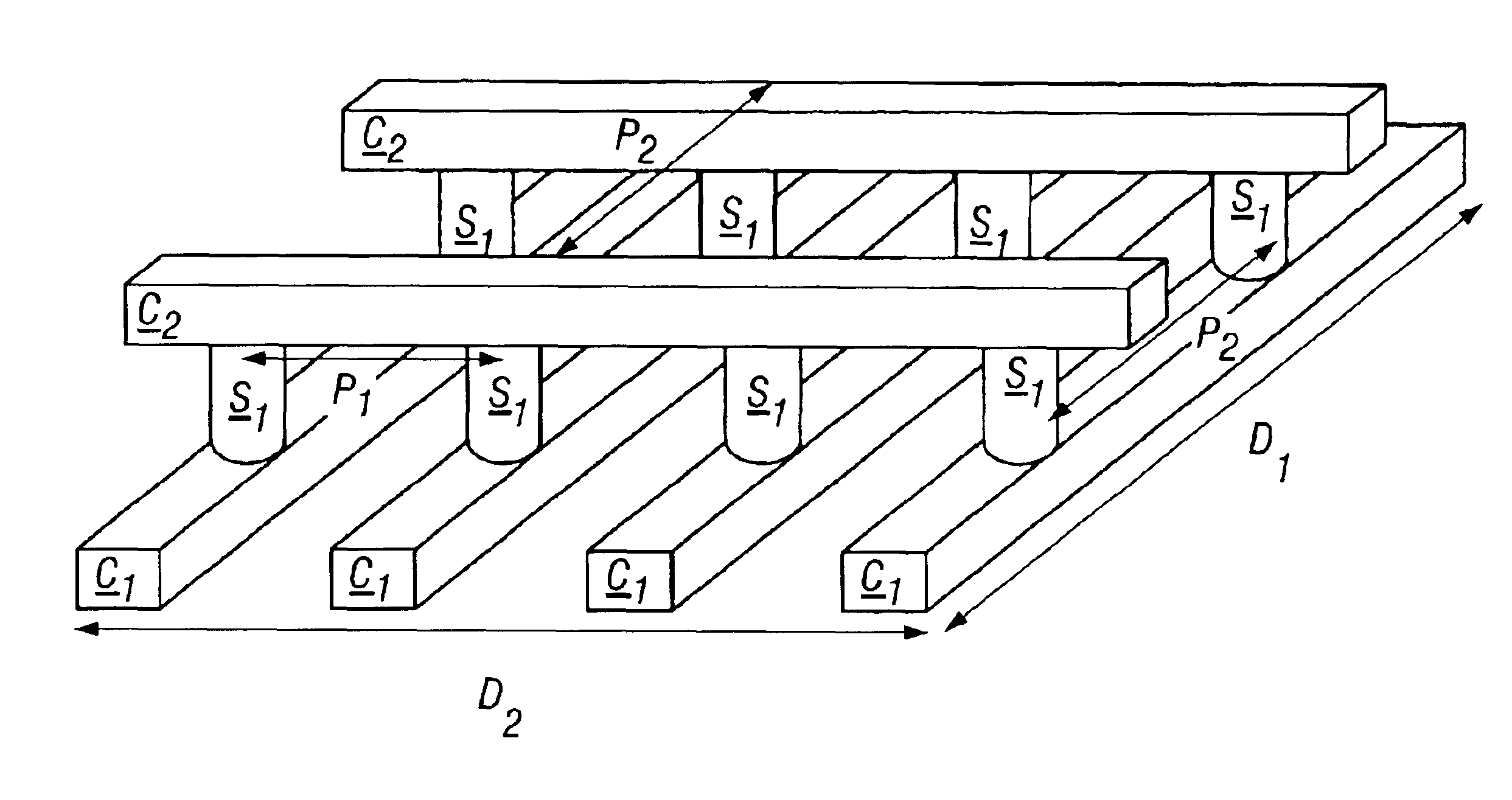
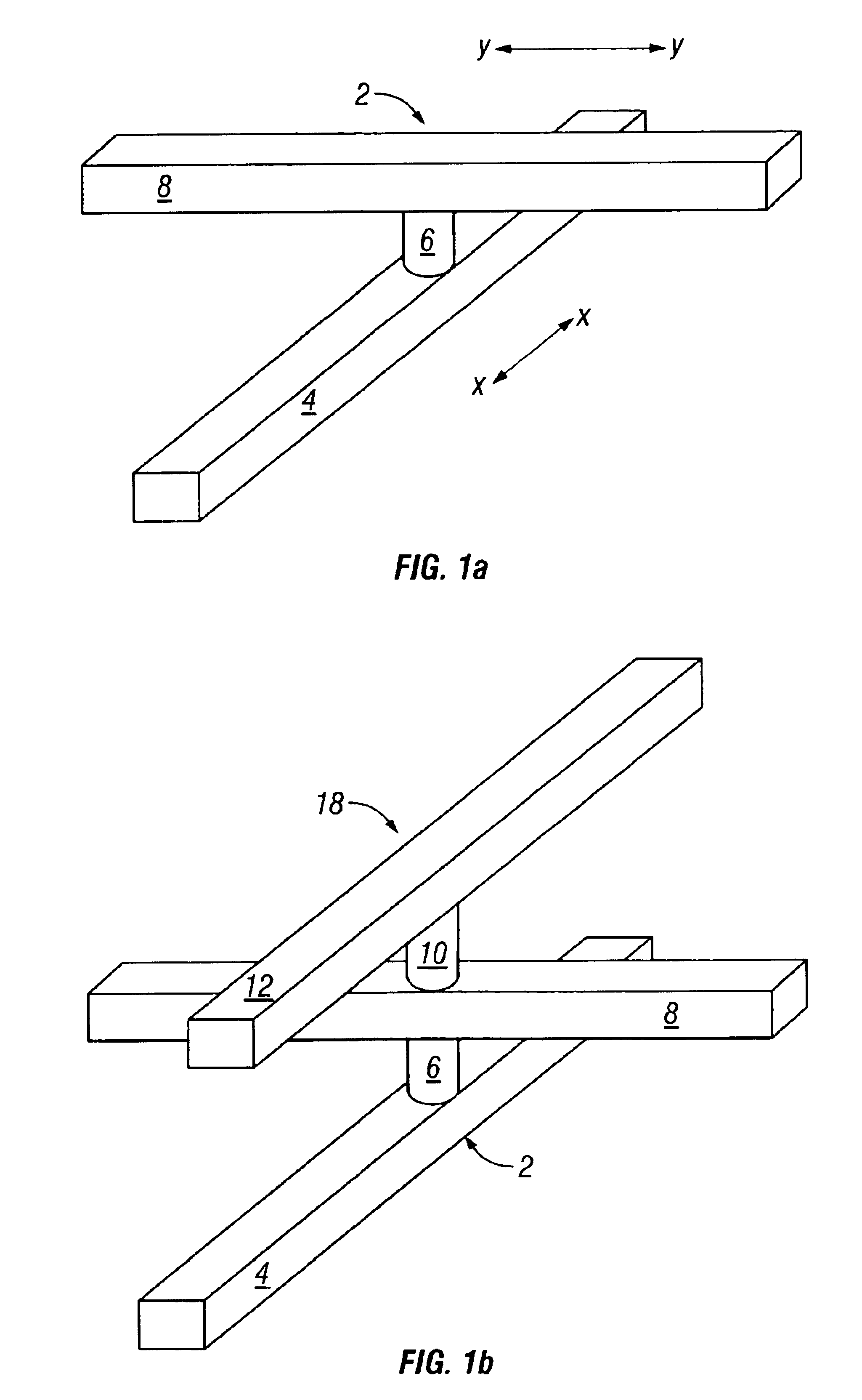
[0122]A detailed description of one preferred embodiment of the preset t invention is provided below. Due to its cylindrical shape, in this description the semiconductor element is referred to as a “beer can.” The bottom story of conductors or “wiring” will be referred to as X1, the one above it as Y2, the one above it as X3, etc. The bottom story of beer cans will be referred to as beer can 1, the one above as beer can 2, etc. This example describes creating a memory array with two stories of memory; memory arrays with more or fewer stories can be created.

[0123]Before creation of the monolithic three dimensional memory above the substrate begins, supporting circuitry, such as complementary metal oxide semiconductor (CMOS) transistors, may be created in the wafer. The steps detailed below begin with wafers processed though completion of CMOS transistors, and referred to as “the front end.” The final step is the routing layer CMP. The routing layer is are the conductive wiring connec...


PUM


Abstract

A three dimensional monolithic memory comprising a memory cell allowing for increased density is disclosed. In the memory cell of the present invention, a bottom conductor preferably comprising tungsten is formed. Above the bottom conductor a semiconductor element preferably comprises two diode portions and an antifuse. Above the semiconductor element are additional conductors and semiconductor elements in multiple stones of memories. The arrangement of processing steps and the choice of materials decreases aspect ratio of each memory cell, improving the reliability of gap fill and preventing etch undercut.

Description

[0001]This application is a continuation of Ser. No. 10 / 326,470 Dec. 19, 2002 abandoned.[0002]This application is a continuation of Herner et al., “An Improved Method for Making High-Density Nonvolatile Memory,” U.S. patent application Ser. No. 10 / 326,470, which is hereby fully incorporated into the instant patent application specification by reference. This application is related to the following applications, all continuations of Ser. No. 10 / 326,470, all filed on even date herewith and all assigned to the assignee of the present invention: Herner et al., “An Improved Method for Making High-Density Nonvolatile Memory,” Ser. No. 10 / 855,775; Vyvoda et al., “Contacts for an Improved High-Density Nonvolatile Memory,” Ser. No. 10 / 855,785; Herner et al., “An Improved Method for Making High-Density Nonvolatile Memory,” Ser. No. 10 / 855,880; Herner et al., “An Improved Method for Making High-Density Nonvolatile Memory,” Ser. No. 10 / 855,804; and Herner et al., “An Improved Method for Making ...

Claims


Application Information

Patent Timeline
Patent Type & Authority Patents(United States)
IPC IPC(8): G11C5/02H01L21/331H01L27/148H01L21/00H01L23/48H01L21/70H01L29/66H01L21/02H01L21/82H01L21/8238H01L31/036H01L31/0392H01L29/94H01L31/115H01L31/119G11CH01L27/102
CPCH01L27/1021H01L21/02518H01L2924/0002H01L2924/00H01L27/148G11C5/02H01L21/8238H01L23/48H01L29/94
Inventor HERNER, S. BRADMAHAJANI, MAITREYEE
Owner SANDISK TECH LLC
Why Eureka
Try Eureka