Manufacturing system and method of semiconductor device

A manufacturing system and semiconductor technology, applied in the fields of simulation equipment, simulation of semiconductor device manufacturing process, and control of manufacturing equipment, can solve problems such as troublesome additional production planning work, increase of wafer inspection processes, and prolonged semiconductor device manufacturing period, etc.

Inactive Publication Date: 2011-01-05
KK TOSHIBA
View PDF2 Cites 4 Cited by
  • Summary
  • Abstract
  • Description
  • Claims
  • Application Information

AI Technical Summary

Problems solved by technology

For this reason, it is necessary to adjust the production plan of semiconductor devices and the number of orders of users, and frequently repeat troublesome additional production planning work, which increases the number of wafer inspection processes and prolongs the manufacturing period of semiconductor devices.

Method used


Image

  • Manufacturing system and method of semiconductor device
  • Manufacturing system and method of semiconductor device
  • Manufacturing system and method of semiconductor device

Examples


no. 8 example

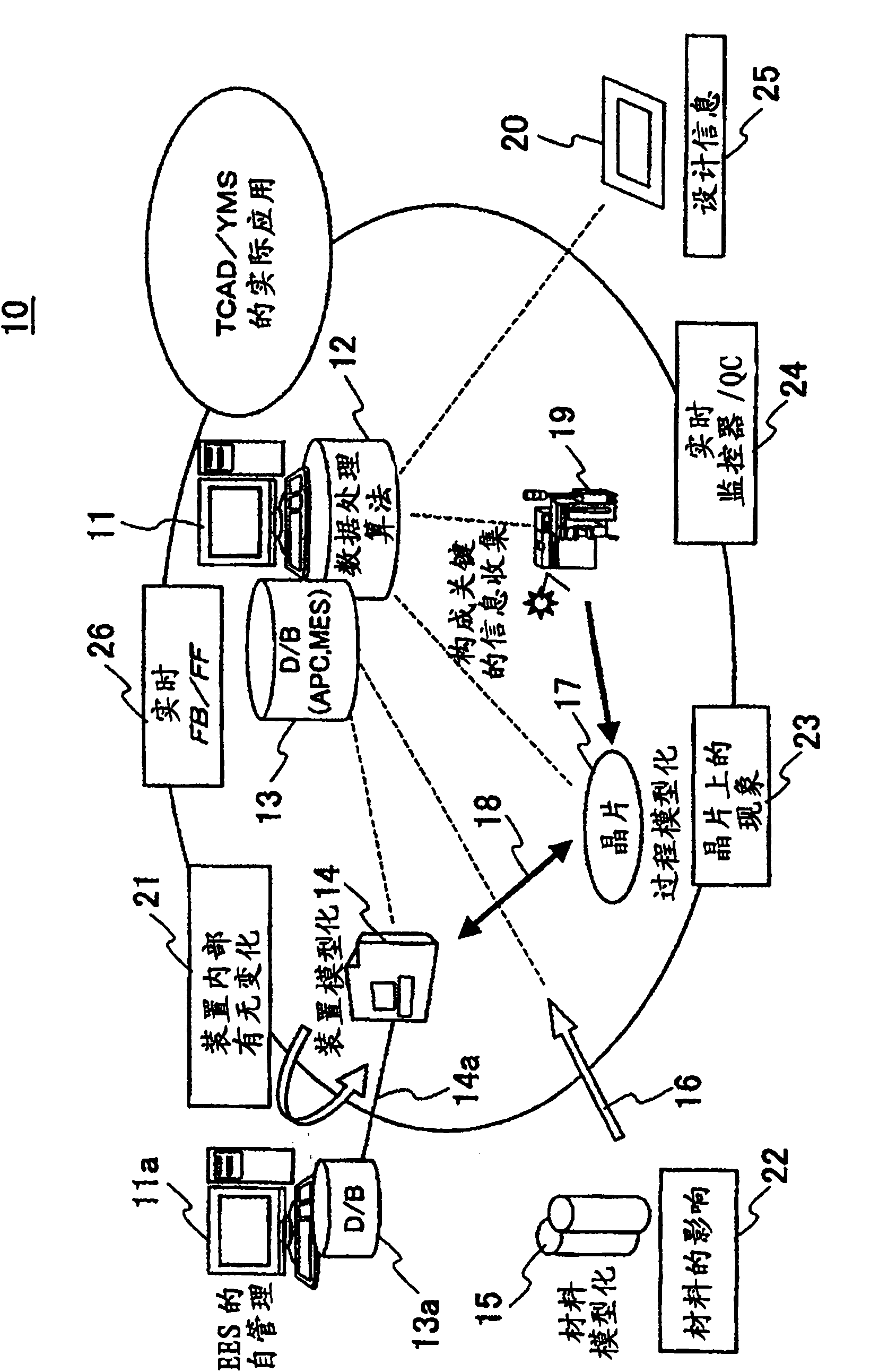
[0155] The semiconductor device manufacturing system of the eighth embodiment of the present invention is as Figure 8 As shown, there is: a processing device 14a for processing a wafer 17a; a processing device 14b for processing a wafer 17b; a processing device 14c for processing a wafer 17c; a processing device 14d for processing a wafer 17d; Devices 5a-5d; databases 13a-13d respectively located in respective diagnostic devices 5a-5d; inspecting devices 19a-19d for inspecting wafers 17a-17d respectively; connected with self-diagnosing devices 5a-5d to receive processing devices 14a-14d A computer 11 of estimated mass values ​​for each of the processed wafers 17a-17d.

[0156] The self-diagnostic means 5a-5d used in the eighth embodiment can be constituted by the same hardware resources as the self-diagnosed system 11a used in the first embodiment and software working in conjunction therewith. In this way, the self-diagnosing devices 5a-5d serving as the self-diagnosing syst...


PUM


Abstract

The present invention relates to a manufacturing system and a method of a semiconductor device. A manufacturing process period of the semiconductor device is shortened by properly managing a maintenance interval of a processing apparatus. This system is provided with a processor (14) for executing process treatment using a semiconductor substrate (17), a self-diagonostic system (11a) for receiving device information from the processor (14) and calculating an estimated quality value of the process treatment, an inspection device (19) for inspecting the result of the process treatment, and a computer (11). The computer (11) compares an inspection result and an estimated quality value, and maintains a parameter of the self-diagonostic system when the estimated quality value is valid and changes a parameter of the self-diagonostic system (11a) when the estimated quality value is invalid.

Description

technical field [0001] The present invention relates to a semiconductor device manufacturing system and a semiconductor device manufacturing method, in particular to a manufacturing device control method, and a semiconductor device manufacturing process simulation method and simulation device using the device and the method. Background technique [0002] Conventionally, semiconductor devices such as DRAMs have been manufactured by using semiconductor manufacturing equipment to repeatedly form substrate steps, form wells, insulate, form transistors, form bit lines, form capacitors, and form wiring. This semiconductor manufacturing process is performed by photolithography treatment, etching treatment, heat treatment (oxidation, annealing, diffusion), ion implantation treatment, or film formation treatment (CVD, sputtering, evaporation), cleaning treatment (resist removal, It consists of a proper combination of solution cleaning) and inspection processing. [0003] In general,...

Claims


Application Information

Patent Timeline
Patent Type & Authority Applications(China)
IPC IPC(8): H01L21/00H01L21/02
CPCG05B19/41875H01L21/67253H01L21/67276H01L22/26H01L22/30
Inventor 牛久幸广柿沼英则秋山龙雄首藤俊次安部正泰小松茂小川章
Owner KK TOSHIBA
Why Eureka
Try Eureka