Fluorescent substance, process for producing same, and luminescent device including same

A technology for a light-emitting device and a manufacturing method, applied in the field of phosphors, capable of solving problems such as increased calorific value, color rendering deviation, and reduced luminous brightness

Active Publication Date: 2012-07-11
NAT INST FOR MATERIALS SCI
View PDF14 Cites 10 Cited by
  • Summary
  • Abstract
  • Description
  • Claims
  • Application Information

AI Technical Summary

Problems solved by technology

[0032] In addition, for light-emitting devices such as lighting, white light-emitting diodes including blue light-emitting diode elements and yttrium-aluminum-garnet-based phosphors have the characteristics of pale light emission due to the lack of red components, and there is color rendering. In addition to the problem of variation, there are also the following problems: In particular, due to the low covalency of oxide phosphors, the luminous luminance decreases due to the increase in the calorific value accompanying the high luminance of semiconductor elements.

Method used


Image

  • Fluorescent substance, process for producing same, and luminescent device including same
  • Fluorescent substance, process for producing same, and luminescent device including same
  • Fluorescent substance, process for producing same, and luminescent device including same

Examples


no. 1 approach

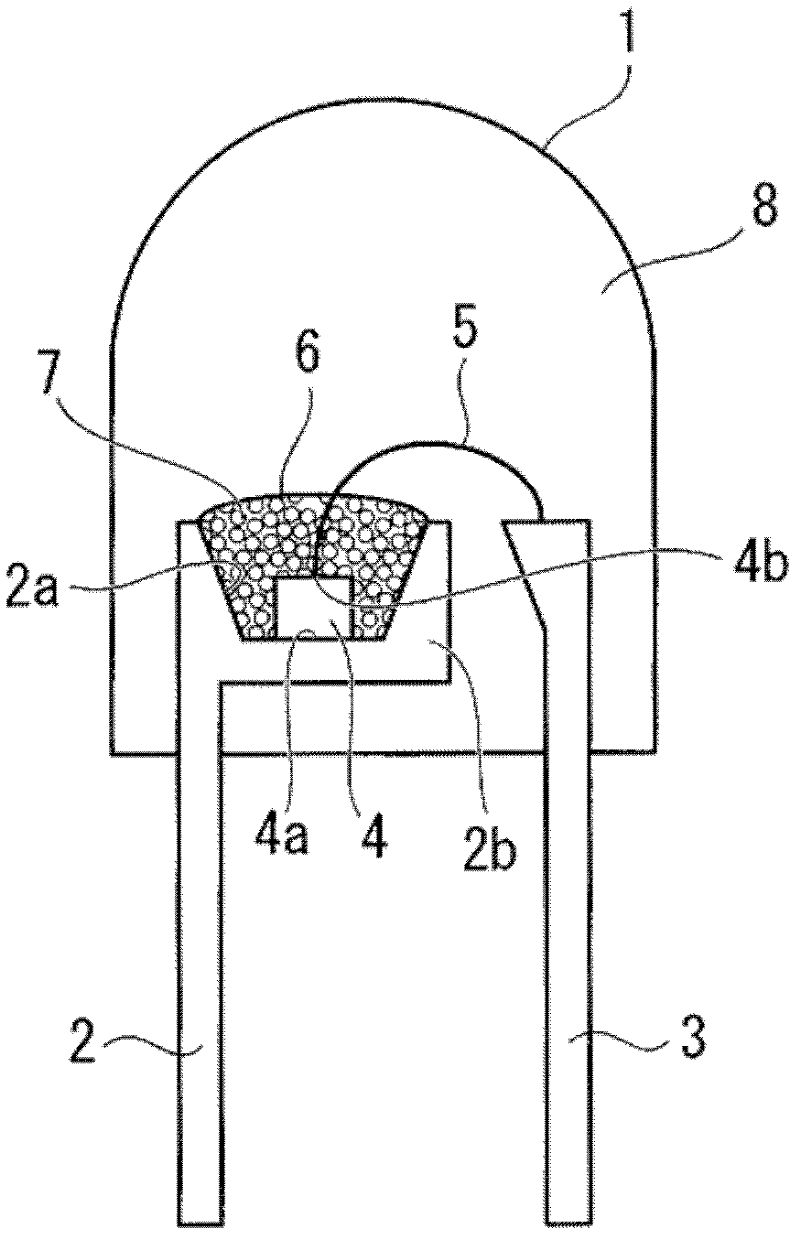
[0239] As a first embodiment of the light-emitting device of the present invention, a cannonball-shaped white light-emitting diode lamp (LED lighting device: LED device) will be described.

[0240] figure 1 It is a cross-sectional view of a cannonball-shaped white light-emitting diode lamp 1 that is a first embodiment of the light-emitting device of the present invention.

[0241] Such as figure 1 As shown, the cannonball-shaped white light-emitting diode lamp 1 has a first lead 2 and a second lead 3, the first lead 2 has a recess 2a, and a light-emitting diode element (LED chip) 4 is built in the recess 2a. In the light emitting diode element 4 , the lower electrode 4 a is electrically connected to the bottom surface of the concave portion 2 a through a conductive paste, and the upper electrode 4 b is electrically connected to the second lead 3 through a bonding wire (fine gold wire) 5 .

[0242] The first resin (encapsulating resin) 6 is a transparent resin in which phosph...

no. 2 approach

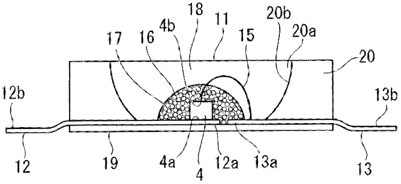
[0249] As a second embodiment of the light-emitting device of the present invention, a chip-type white light-emitting diode lamp for substrate mounting (LED lighting device: LED device) will be described.

[0250] figure 2 It is a cross-sectional view of a chip-type white light-emitting diode lamp 11 for substrate mounting that is a second embodiment of the light-emitting device of the present invention.

[0251] Such as figure 2 As shown, the chip-type white light-emitting diode lamp 11 for substrate mounting is fixed with a first lead 12 and a second lead 13 on a ceramic substrate 19 made of white alumina ceramics with high reflectance of visible light. 13a is located in the approximate center of the substrate 19, and the ends 12b and 13b on the opposite side protrude to the outside, respectively, and serve as electrodes to be soldered when mounted on the electric substrate. The end 12 a of the first lead 12 is fixed with a built-in light emitting diode element (LED chip...

no. 3 approach

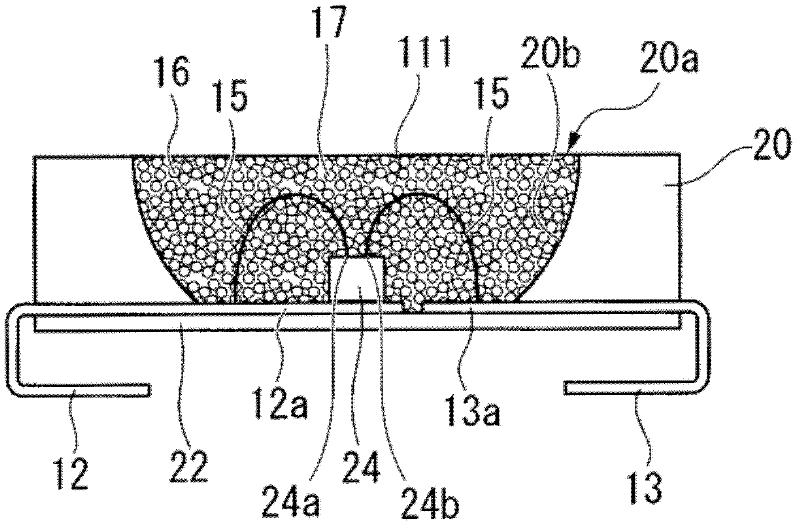
[0259] As a second embodiment of the light-emitting device of the present invention, a chip-type white light-emitting diode lamp for substrate mounting (LED lighting device: LED device) will be described.

[0260] image 3 It is a cross-sectional view of a chip-type white light-emitting diode lamp 111 for substrate mounting that is a third embodiment of the light-emitting device of the present invention.

[0261] Such as image 3 As shown, the chip-type white light-emitting diode lamp 111 for substrate mounting is fixed with a first lead 12 and a second lead 13 on a ceramic substrate 19 made of white alumina ceramics with high reflectance of visible light. 13a is located in the approximate center of the substrate 19, and the ends 12b and 13b on the opposite side protrude to the outside, respectively, and serve as electrodes to be soldered when mounted on the electric substrate. The end 12 a of the first lead 12 is fixed by incorporating a light emitting diode element (LED ch...


PUM

PropertyMeasurementUnit
particle sizeaaaaaaaaaa
luminescence spectroscopyaaaaaaaaaa
thicknessaaaaaaaaaa

Abstract

Provided are a fluorescent substance represented by the general formula (A1-xRxM2X)m(M2X4)n, a process for producing the fluorescent substance, and a luminescent device including the fluorescent substance. (In the formula, element A is one or more elements selected from Li, Na, Be, Mg, Ca, Sr, Ba, Sc, Y, La, Gd, and Lu; element R is one or more elements selected from Mn, Ce, Pr, Nd, Sm, Eu, Tb, Dy, Ho, Er, Tm, and Yb; element M is one or more elements selected from Si, Ge, Sn, Ti, Hf, Zr, Be, B, Al, Ga, In, Tl, and Zn; element X is oxygen and/or nitrogen; n and m each is an integer of 1 or larger; and x is a real number of 0 < x <1.)

Description

technical field [0001] The present invention relates to a phosphor mainly composed of an inorganic compound and its use. More specifically, this application relates to light-emitting devices such as lighting devices and display devices utilizing the property of the phosphor, that is, the characteristic of emitting fluorescence with a long wavelength of 400 nm or more. [0002] This application claims priority based on Patent Application No. 2009-183313 for which it applied to Japan on August 6, 2009, The content is used for this application. Background technique [0003] In general, phosphors are used in display devices such as fluorescent display tubes (VFDs), field emission displays (FEDs), plasma display panels (PDPs), cathode ray tubes (CRTs), and light-emitting diodes (LED elements). light emitting device. [0004] In any of these light-emitting devices, in order to cause the phosphor to emit light, it is necessary to supply some energy to the phosphor in order to exc...

Claims


Application Information

Patent Timeline
Patent Type & Authority Applications(China)
IPC IPC(8): C09K11/64C09K11/80H01L33/50
CPCH01L2224/48091H01L24/45H01L2224/48247H01L2224/8592C09K11/7721H01L24/48H01L33/502H01L2224/45144C09K11/7734H01L2924/15747H01L2924/12042H01L2924/12036H01L2924/12041H01L2924/181C09K11/77348H01L2924/00014H01L2924/00H01L2924/00012C09K11/55C09K11/77C09K11/64
Inventor 盐井恒介广崎尚登道上勇一
Owner NAT INST FOR MATERIALS SCI
Why Eureka
Try Eureka