
Wafer-level packaging method and packaging structure thereof
A wafer-level packaging and wafer technology, which is applied in the manufacturing of electrical components, electrical solid-state devices, semiconductor/solid-state devices, etc., can solve the problems of low input and output port density, large package volume, poor reliability, etc. , The effect of small package size and thin package thickness
- Summary
- Abstract
- Description
- Claims
- Application Information
AI Technical Summary
Problems solved by technology
Method used
Image

Examples
Embodiment Construction
[0030] Specific embodiments of the present invention will be described in detail below in conjunction with the accompanying drawings.
[0031] In one embodiment of the wafer level packaging method involved in the present invention, it comprises the following steps:
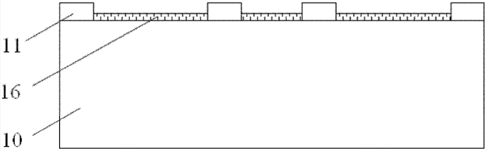
[0032] First, a wafer 10 comprising chip units (not shown) is provided; see figure 1 , carry out bumping process (Bumping) and secondary passivation treatment on the front side of the wafer; where the bumping process can use known methods in the industry such as electroplating, sputtering or chemical replacement, and copper, nickel, antimony, gold or Bumps 11 of materials such as tin are grown on the front of the wafer; and the secondary passivation treatment generally involves growing a secondary passivation layer 16 on the front of the wafer, wherein the secondary passivation layer can be a polyimide film, etc. ;
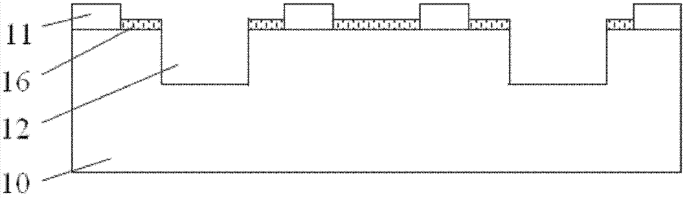
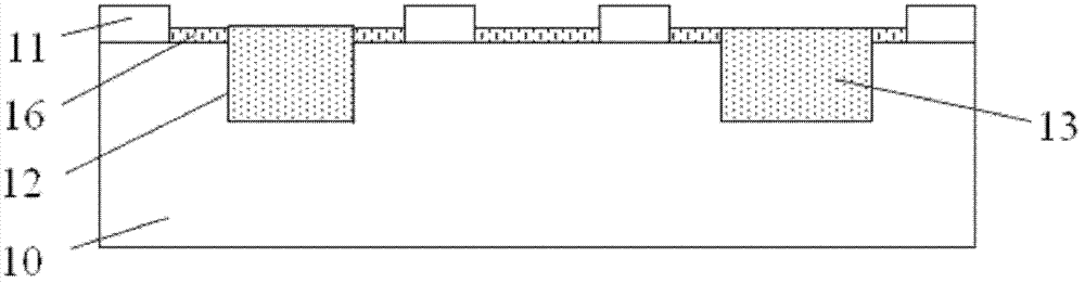
[0033] Please refer to figure 2 A first groove 12 is opened between adjacent bumps 11 of adjac...
PUM
 Abstract
Description
Claims
Application Information