Wafer-level packaging method based on si conductive pillars and its monolithic integrated mems chip

A technology of wafer-level packaging and MEMS structure layer, which is applied in the direction of circuits, electrical components, and electric solid-state devices, can solve the problems of high cost, complicated process, and affecting the performance of MEMS devices, and achieve low cost, simple manufacturing process, and anti-corrosion. The effect of strong environmental interference ability

Active Publication Date: 2015-10-28
ANHUI BEIFANG XINDONG LIANKE MICROSYST TECH
View PDF6 Cites 1 Cited by
  • Summary
  • Abstract
  • Description
  • Claims
  • Application Information

AI Technical Summary

Problems solved by technology

However, the process of forming through-Si via (TSV) conductive pillars on this chip is complicated and costly
Moreover, the position of the solder ball is relatively close to the MEMS structure. During the subsequent secondary packaging, the package stress will be transmitted to the MEMS structure through the solder ball, which will affect the performance of the MEMS device.

Method used


Image

  • Wafer-level packaging method based on si conductive pillars and its monolithic integrated mems chip
  • Wafer-level packaging method based on si conductive pillars and its monolithic integrated mems chip
  • Wafer-level packaging method based on si conductive pillars and its monolithic integrated mems chip

Examples


Embodiment 1

[0045] (1) MEMS wafer formation:

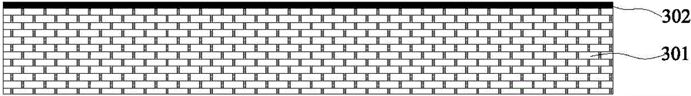
[0046] Oxidize the cover plate 301 to generate a cover plate insulating layer 302, such as image 3 As shown, the material of the cover plate 301 is single crystal Si heavily doped with boron, and the resistivity is about 0.01 Ω·cm, so the material of the cover plate insulating layer 302 is SiO 2 ; Glue coating, exposure, development, etching, deglue and other semiconductor processing techniques on the cover insulating layer 302 to form a cover cavity 306a on the front of the cover 301, such as Figure 4 As shown; the MEMS structure layer 303 is bonded and annealed with the cover plate 301 with the upper cavity, and the MEMS structure layer 303 is thinned to the required thickness by grinding, as Figure 5 As shown, the material of the MEMS structure layer is single crystal Si heavily doped with boron; on the MEMS structure layer 303, a deep hole 305 is etched through standard semiconductor processing steps, and in the deep hole 305, the cov...

Embodiment 2

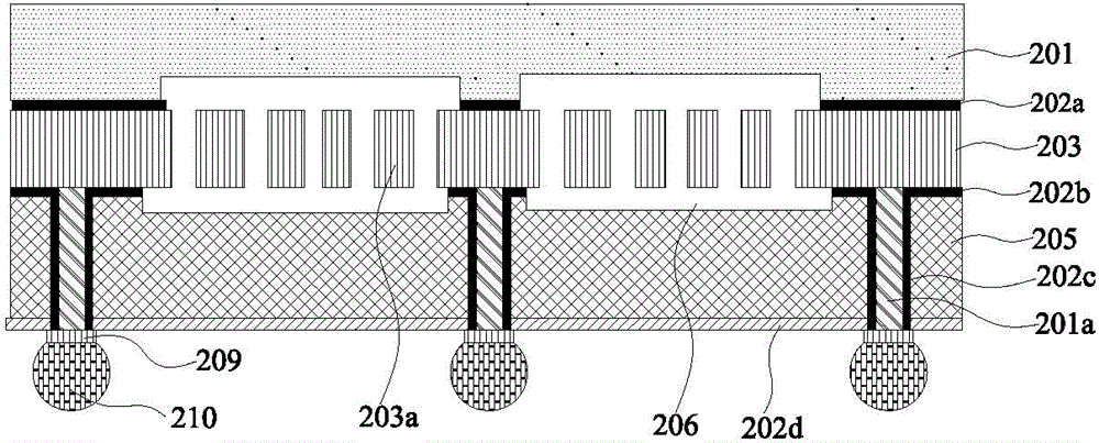
[0061] The difference between this embodiment and Embodiment 1 lies in the forming steps of the monolithic integrated MEMS chip. The monolithic integrated MEMS chip of this embodiment is formed as follows: plant solder balls 310 on metal solder bumps 309, and then Deep grooves 308 on the outside cut the composite wafer to form Figure 16 The monolithic integrated MEMS chip used for common packaging shown in the present embodiment can be directly flip-chip welded on the user's PCB board for use.

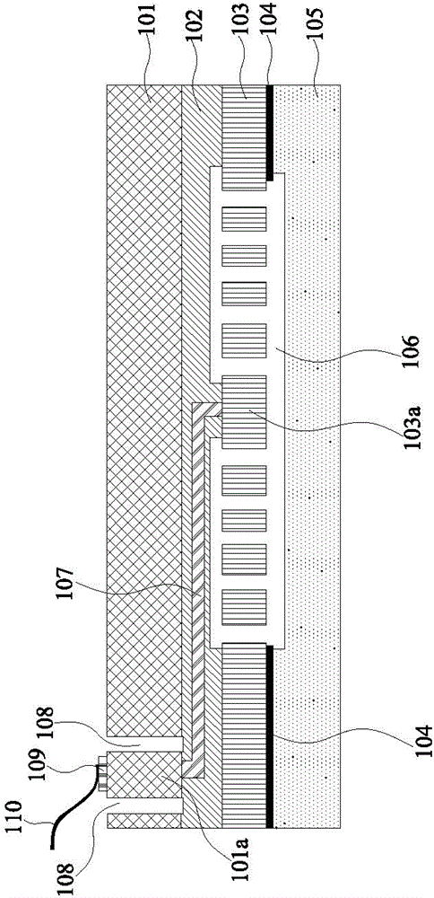
[0062] The monolithic integrated MEMS chip that present embodiment makes, as Figure 16 As shown, it is formed by bonding a cover plate 301, a MEMS structure layer 303 and an ASIC chip 400. The material of the cover plate 301 is a heavily doped Si sheet, and its resistivity is about 0.01 Ω·cm, which is a good conductive material. The MEMS structure layer 303 is divided into a MEMS structure 303a and a MEMS conductive block 303b. The MEMS structure 303a is a movable part of the MEMS s...


PUM


Abstract

The invention discloses a Si conductive post based wafer-level packaging method and a monolithic integrated MEMS (Micro Electro Mechanical System) chip for the same. The method comprises the steps of forming an MEMS wafer; forming an ASIC (Application Specific Integrated Circuit) wafer to be bonded; forming a monolithic integrated MEMS wafer; forming a Si conductive post; forming a monolithic integrated MEMS chip. The chip disclosed by the invention is formed by bonding the MEMS wafer and the ASIC wafer to be bonded, an upper cavity of a cover plate, a lower cavity of the ASIC chip and an MEMS structural layer are defined to form a sealing cavity, and an MEMS structure is located in the sealing cavity; a cover plate insulating layer is arranged between the cover plate and the MEMS structural layer, and the cover plate is provided with a conductive post which is connected with a metal welding block and a conductive stopper; the ASIC wafer to be bonded comprises a metal sealing layer, a first metal layer and a second metal layer, wherein the first metal layer is electrically connected with the second metal layer, and the second metal layer located in the sealing cavity is used as a lower electrode to induct the motion of the MEMS structure. The method is simple in operation, the prepared chip is small in size and low in cost, and an environment interference signal and a packaging stress have little influence to the performance of an MEMS device.

Description

technical field [0001] The invention belongs to the field of chip packaging, and in particular relates to a monolithic integrated MEMS chip, and also relates to a wafer-level packaging method for the MEMS chip. Background technique [0002] Electronic packaging is to electrically connect one or more electronic chips to each other, and then encapsulate them in a protective structure, the purpose of which is to provide electrical connection, mechanical protection or chemical corrosion protection for electronic chips. However, for some electronic products, the surface of the chip cannot be in contact with the packaging material, especially some micro sensors, such as MEMS devices, surface acoustic wave / bulk acoustic wave filters, oscillators, etc., need to be sealed with ceramic shells, metal shells or plastic shells, etc. Hermetic packaging, but these packaging methods are costly and bulky, making them unsuitable for use in consumer electronics. The development trend of packa...

Claims


Application Information

Patent Timeline
Patent Type & Authority Patents(China)
IPC IPC(8): H01L21/56
CPCH01L2224/11
Inventor 华亚平
Owner ANHUI BEIFANG XINDONG LIANKE MICROSYST TECH
Why Eureka
Try Eureka