Circuit width thinning defect prevention device and method of preventing circuit width thinning defect

A technology for changing circuit width and devices, which is applied to printed circuits, measuring devices, and chemical/electrolytic methods to remove conductive materials, etc., and can solve problems such as circuit width thinning

Active Publication Date: 2014-07-09
SAMSUNG ELECTRO MECHANICS CO LTD
View PDF4 Cites 0 Cited by
  • Summary
  • Abstract
  • Description
  • Claims
  • Application Information

AI Technical Summary

Problems solved by technology

[0017] This circuit width narrowing defect according to the reduction of circuit width has become a serious problem

Method used


Image

  • Circuit width thinning defect prevention device and method of preventing circuit width thinning defect
  • Circuit width thinning defect prevention device and method of preventing circuit width thinning defect
  • Circuit width thinning defect prevention device and method of preventing circuit width thinning defect

Examples


Embodiment Construction

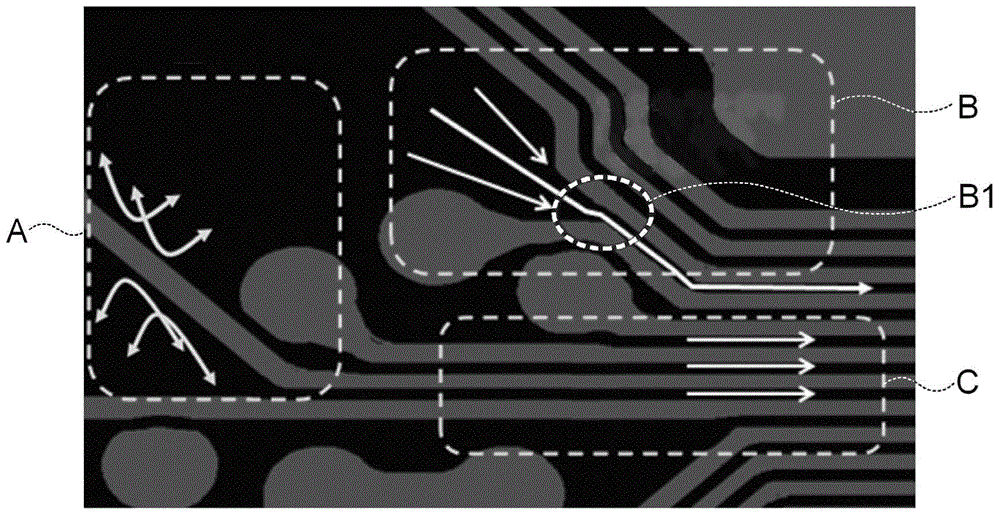
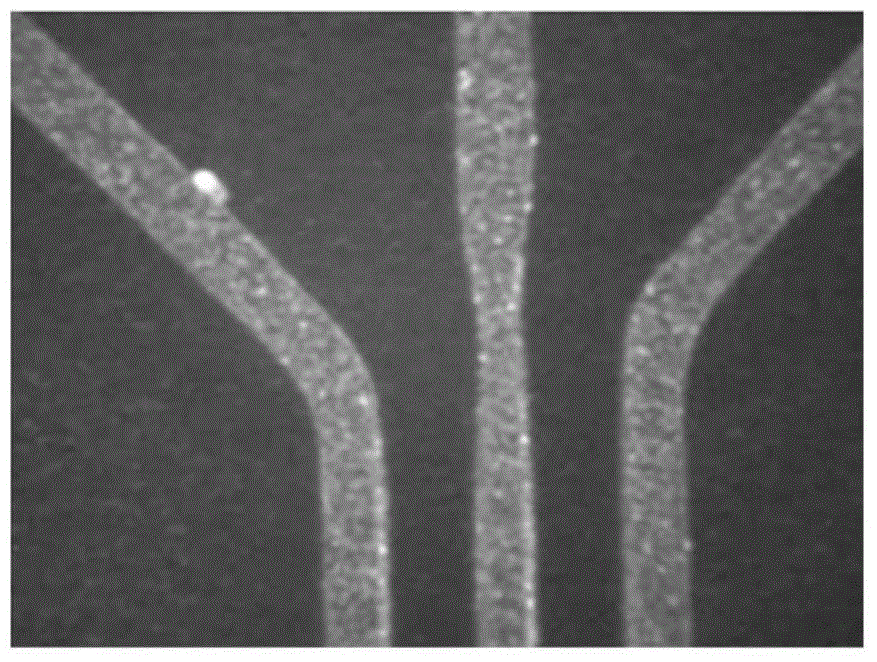
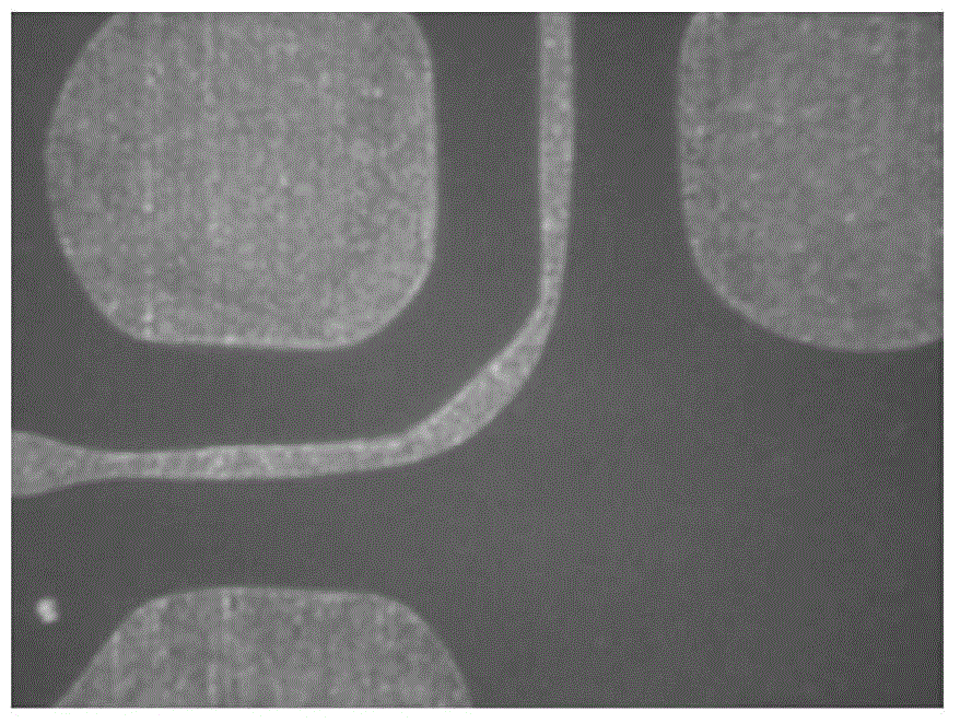
[0042] The advantages and features of the present invention and the method for realizing the present invention will be apparent by referring to the following embodiments described in detail with reference to the accompanying drawings. However, the present invention is not limited to the embodiments disclosed below and may be implemented in various forms. These embodiments are provided only to complete the disclosure of the invention and to fully convey the scope of the invention to those skilled in the art. Throughout this specification, the same reference numerals refer to the same elements.

[0043] The terms used herein are used to describe the embodiments, not to limit the present invention. Throughout this specification, unless the context clearly indicates otherwise, the singular form includes the plural form, and the term "comprises" and / or "comprises" used herein does not exclude other than the above-mentioned components, steps, operations and / or means. The presence ...


PUM


Abstract

The present invention relates to a circuit width thinning defect prevention device and a method of preventing a circuit width thinning defect, and can prevent a circuit width thinning defect, that is, a reduction in circuit width due to excessive etching on a specific portion by including a storage means for storing dam design information classified according to the type of a weak portion; an analysis means for analyzing first design information to deduce the type and position of the weak portion; a matching means for extracting the dam design information corresponding to the type of the weak portion from the dam design information stored in the storage means; and a change means for changing the first design information to add a dam according to the dam design information extracted by the matching means to the position of the weak portion deduced by the analysis means.

Description

[0001] Cross References to Related Applications [0002] This application claims the benefit of Korean Patent Application No. 10-2012-0158336 filed on December 31, 2012, the entire contents of which are incorporated herein by reference. technical field [0003] The invention relates to a circuit width narrowing defect prevention device and a method for preventing circuit width narrowing defects. Background technique [0004] One method widely used in the field of printed circuit boards is the capping method. [0005] The capping method is a method of forming a circuit pattern by forming a resist pattern on the surface of a conductive layer using a dry film etc. The conductive layer in the region outside the resist pattern), and the resist pattern is removed, and this capping method is introduced in many documents such as Patent Document 1. [0006] Recently, with increasing demand for slimming and miniaturization and high performance of electronic devices, fine patterns ar...

Claims


Application Information

Patent Timeline
Patent Type & Authority Applications(China)
IPC IPC(8): H05K3/06
CPCG06F30/398G01B11/046G01B2210/58G01N2021/95638H05K13/08H05K2203/163
Inventor 成定庆丘奉完赵元佑
Owner SAMSUNG ELECTRO MECHANICS CO LTD
Why Eureka
Try Eureka