Optical imaging lens and electronic device applying optical imaging lens

An optical imaging lens and imaging technology, applied in the field of optical lenses, can solve problems such as unfavorable thinning of portable electronic products, and achieve the effect of light, thin, short and miniaturized structure design, good practical performance, and overcoming aberrations

Active Publication Date: 2015-07-29
GENIUS ELECTRONICS OPTICAL XIAMEN
View PDF7 Cites 12 Cited by
  • Summary
  • Abstract
  • Description
  • Claims
  • Application Information

AI Technical Summary

Problems solved by technology

[0003] The known optical imaging lenses are mostly four-piece optical imaging lenses. Due to the small number of lenses, the length of optical imaging lenses can be shortened. However, with the increasing demand for high-standard products, optical imaging lenses are used in The demand for picture quality and quality is rapidly increasing, and it is extremely necessary to develop products with higher specifications,

Method used


Image

  • Optical imaging lens and electronic device applying optical imaging lens
  • Optical imaging lens and electronic device applying optical imaging lens
  • Optical imaging lens and electronic device applying optical imaging lens

Examples


Embodiment Construction

[0123] The present invention will be further described in conjunction with the accompanying drawings and specific embodiments. Before the present invention is described in detail, it should be noted that in the following description, similar components are denoted by the same numerals.

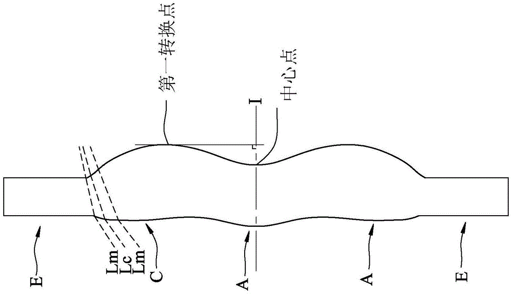
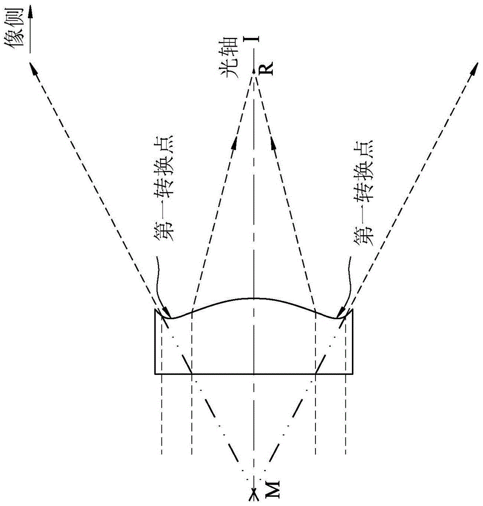
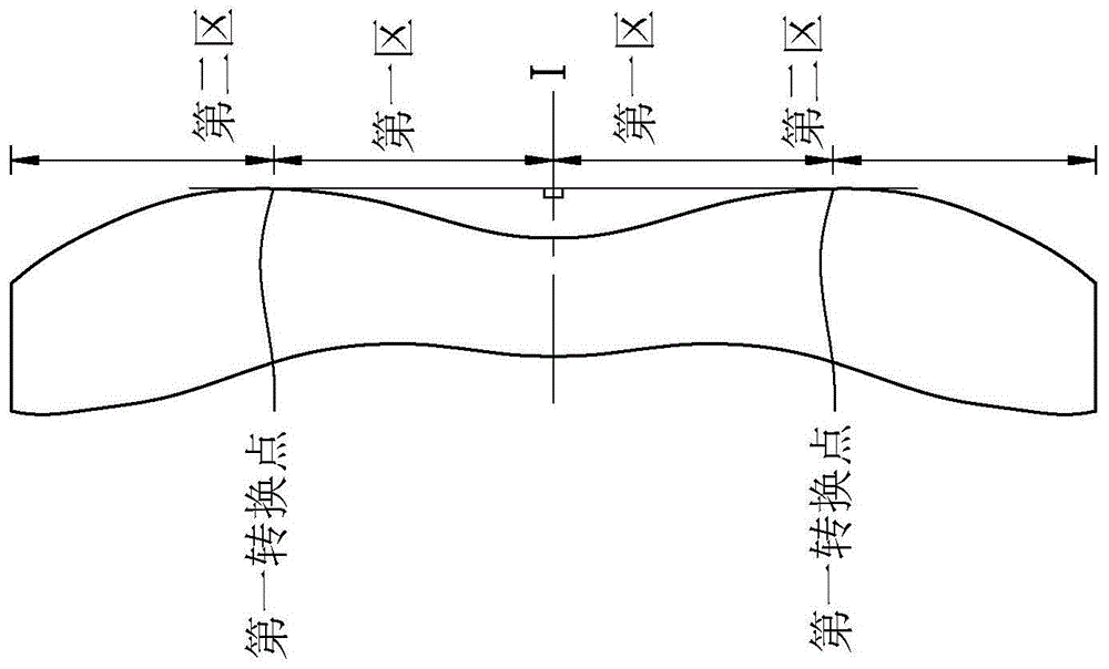
[0124] The term "a lens has positive (or negative) refractive power" in this specification refers to the positive (or negative) refractive power of the lens on the optical axis calculated by Gaussian optics theory. The image side and object side are defined as the range through which the imaging light passes, where the imaging light includes the chief ray Lc and the marginal ray Lm, such as figure 1 As shown, I is the optical axis and this lens is radially symmetrical to each other with the optical axis I as the symmetry axis. The area where the light rays pass through the optical axis is the area A near the optical axis, and the area where the marginal light rays pass is the area C near the c...


PUM


Abstract

The invention relates to an optical imaging lens and an electronic device applying the optical imaging lens. The optical imaging lens comprises six lenses and is characterized in that an object side surface of the first lens is provided with a convex surface portion located in an area nearby the circumference; the second lens is made of plastic; an image side surface of the third lens is provided with a concave surface portion located in an area nearby an optical axis; the fourth lens is provided with a positive refractive index, an object side surface of the fourth lens is provided with a concave surface portion located in an area nearby the circumference, and an image side surface of the fourth lens is provided with a concave surface portion located in an area nearby the circumference; an image side surface of the fifth lens is provided with a convex surface portion located in an area nearby the optical axis; and an object side surface of the sixth lens is provided with a convex surface portion located in an area nearby the optical axis, and the sixth lens is made of the plastic. The electronic device comprises a casing and an image module, wherein the image module is installed in the casing and comprises the optical imaging lens, a lens cone, a module rear base unit and an image sensor. The optical imaging lens and the electronic device applying the optical imaging lens are enabled to have good practical performance, and thin and short structural design is facilitated.

Description

technical field [0001] The invention relates to an optical lens, in particular to an optical imaging lens and an electronic device using the optical imaging lens. Background technique [0002] In recent years, the popularization of portable electronic products such as mobile phones and digital cameras has led to the vigorous development of imaging module related technologies. The imaging module mainly includes components such as optical imaging lens, module holder unit and sensor. The thin and light trend of digital cameras also makes the miniaturization of image modules more and more demanding. For the technological progress and size reduction of CMOS), the length of the optical imaging lens loaded in the image module also needs to be shortened accordingly. performance. However, the most important characteristics of optical imaging lenses are nothing more than imaging quality and volume. [0003] The known optical imaging lenses are mostly four-piece optical imaging lens...

Claims


Application Information

Patent Timeline
IPC IPC(8): G02B13/18G02B13/00G02B7/02
CPCG02B9/62G02B13/0045G02B13/06G02B13/18G02B13/00H04N23/00
Inventor 陈思翰张加欣谢宏健
Owner GENIUS ELECTRONICS OPTICAL XIAMEN
Why Eureka
Try Eureka