Silicon nitride waveguide calorescence switch array chip based on Mach-Zahnder structure and production method thereof

An optical switch array, silicon nitride wave technology, applied in optics, nonlinear optics, instruments, etc., can solve the problems of complex manufacturing process, complex processing technology, large device size, etc., and achieve simple process flow, low transmission loss, Small device size effect

Inactive Publication Date: 2015-08-19
SOUTHEAST UNIV
View PDF4 Cites 30 Cited by
  • Summary
  • Abstract
  • Description
  • Claims
  • Application Information

AI Technical Summary

Problems solved by technology

The silicon dioxide-based waveguide thermo-optic switch array has a small difference in refractive index between the core layer and the cladding layer of the optical waveguide, and the bending radius of the optical waveguide is large, resulting in a large device size, which is not conducive to high-density integration, and the thermo-optic coefficient of the material is small. The power consumption is high, and its manufacturing process is complicated and the cost is high; in the waveguide thermo-optical switch array based on silicon dioxide based on silicon dioxide, the refractive ind...

Method used


Image

  • Silicon nitride waveguide calorescence switch array chip based on Mach-Zahnder structure and production method thereof
  • Silicon nitride waveguide calorescence switch array chip based on Mach-Zahnder structure and production method thereof
  • Silicon nitride waveguide calorescence switch array chip based on Mach-Zahnder structure and production method thereof

Examples


Embodiment Construction

[0035] The present invention will be further described below in conjunction with the accompanying drawings.

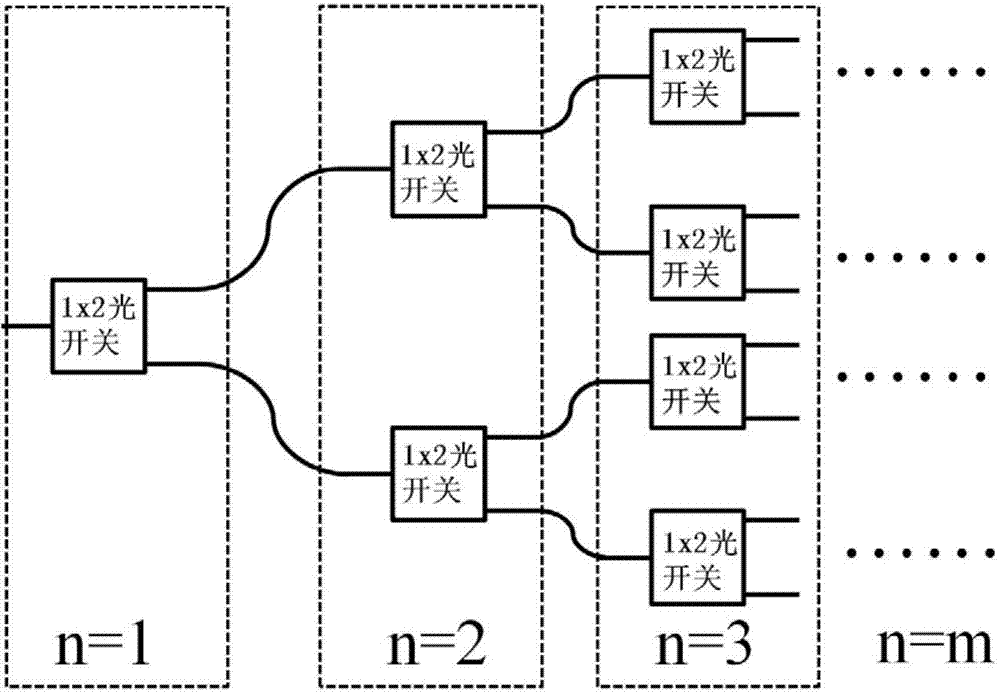
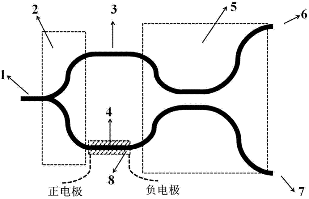
[0036] Such as figure 1 Shown is a specific implementation schematic diagram of a silicon nitride waveguide thermo-optic switch array chip based on the Mach-Zehnder structure of the present invention, wherein each 1×2 Mach-Zehnder type silicon nitride waveguide thermo-optic switch unit is as figure 2 shown.

[0037] A silicon nitride waveguide thermo-optic switch array chip based on Mach-Zehnder structure, which is composed of multiple cascaded 1×2 Mach-Zehnder silicon nitride waveguide thermo-optic switch units, each of which is 1×2 Mach -Zehnder-type silicon nitride waveguide thermo-optical switch unit includes an input optical waveguide 1, a 1×2 branch optical waveguide 2, a reference arm optical waveguide 3, an interference arm optical waveguide 4, and a 3dB directional coupler 5. Two output optical waveguides, respectively the first output optical waveguide 6 a...


PUM

PropertyMeasurementUnit
Resistivityaaaaaaaaaa
Thicknessaaaaaaaaaa

Abstract

The invention discloses a silicon nitride waveguide calorescence switch array chip based on a Mach-Zahnder structure and a production method thereof. The chip comprises a plurality of cascaded 1*2 Mach-Zahnder silicon nitride waveguide calorescence switch units; each unit comprises an input optical waveguide, an 1*2 branch optical waveguide, a reference arm optical waveguide, a 3dB directional coupler and two output optical waveguides. The chip is small in size, low in consumption, simple in machining process, compatible with the semiconductor CMOS process, low in cost and easy to integrate, and the application prospect in the fields of optical communication and optical interconnection is promised.

Description

technical field [0001] The invention belongs to the technical field of integrated waveguide optical switch arrays, in particular to a silicon nitride waveguide thermo-optical switch array chip based on a Mach-Zehnder structure and a manufacturing method thereof. Background technique [0002] Integrated waveguide optical switch array is an integrated photonic device that controls light on and off. It is widely used in optical cross multiplexing in optical communication systems, protection switching systems in optical networks, and real-time monitoring systems for network performance. , Light source control, light sensor system, etc. in the test of optical devices. The working mechanism of the waveguide thermo-optic switch based on the Mach-Zehnder structure is generally to use the thermo-optic effect to change the refractive index of the optical waveguide medium, thereby changing the phase difference between the reference arm and the interference arm in the Mach-Zehnder inter...

Claims


Application Information

Patent Timeline
IPC IPC(8): G02F1/01
CPCG02F1/0147G02F2201/06G02F2202/10
Inventor 恽斌峰胡国华张若虎钟嫄崔一平
Owner SOUTHEAST UNIV
Why Eureka
Try Eureka