Thin film transistor, array substrate and display device

A technology of thin film transistors and array substrates, applied in the field of liquid crystal display, can solve the problems of reducing the performance of thin film transistors, difficult channel, large aspect ratio, etc., and achieves the effect of ensuring display quality, improving resolution, and large aspect ratio.

Active Publication Date: 2015-11-25
BOE TECH GRP CO LTD
View PDF4 Cites 9 Cited by
  • Summary
  • Abstract
  • Description
  • Claims
  • Application Information

AI Technical Summary

Problems solved by technology

[0003] With the continuous development of display technology, users have higher and higher requirements for resolution, which inevitably requires higher aperture ratio and smaller TFT size. For small-sized TFTs, it is difficult to achieve a larger channel. aspect ratio, reducing the performance of thin film transistors

Method used


Image

  • Thin film transistor, array substrate and display device
  • Thin film transistor, array substrate and display device
  • Thin film transistor, array substrate and display device

Examples


Embodiment Construction

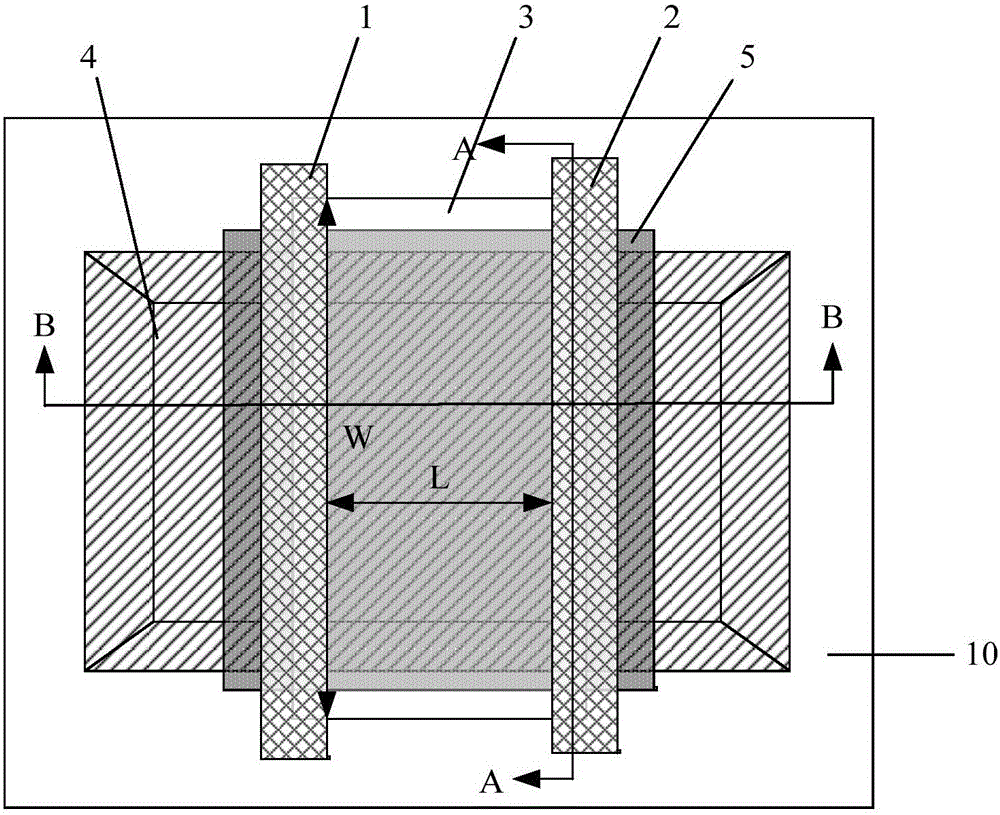
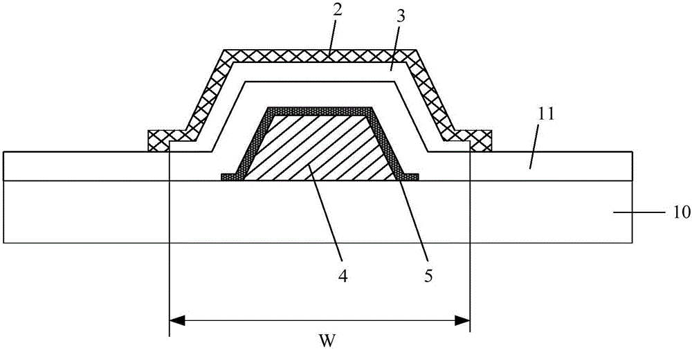
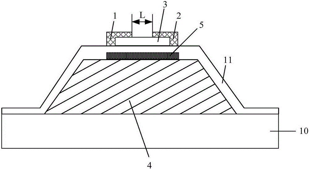
[0034] As the resolution of thin film transistor liquid crystal display becomes higher and higher, higher aperture ratio and smaller size of thin film transistor are bound to be required. For a thin film transistor with a small size, it is difficult to achieve a larger width-to-length ratio in the channel, which reduces the performance of the thin film transistor.

[0035] In order to solve the above-mentioned technical problems, the present invention provides a thin film transistor, which includes a source electrode, a drain electrode, and a pattern of an active layer disposed on a base substrate, and the active layer is located at a portion between the source electrode and the drain electrode. form channels. In the direction perpendicular to the surface of the base substrate, the broadside profile of the channel is set to have a curve segment that fluctuates up and down in a curve, so that when the projected area of ​​the thin film transistor on the base substrate is constan...


PUM


Abstract

The invention relates to the technical field of liquid crystal display, and discloses a thin film transistor, an array substrate and a display device. The thin film transistor is arranged on a substrate base plate; in the direction vertical to the surface of the substrate base plate, the broadside outline of a channel of the thin film transistor comprises a curved section which changes up and down in a curved line, so that the width-to-length ratio of the channel can be increased under the condition that the projection area of the thin film transistor on the substrate base plate is fixed; the firing current of the thin film transistor is increased; and the performance of the thin film transistor is improved. Meanwhile, the performance of the thin film transistor can be ensured; the size of the thin film transistor is reduced; the resolution ratio of the display device is increased; and the display quality is ensured.

Description

technical field [0001] The invention relates to the technical field of liquid crystal display, in particular to a thin film transistor, an array substrate and a display device. Background technique [0002] Thin Film Transistor-Liquid Crystal Display (TFT-LCD) has the characteristics of small size, low power consumption, and no radiation. It has developed rapidly in recent years and occupies a dominant position in the current flat panel display market. The array substrate is one of the main structures of the thin film transistor-LCD, including gate lines and data lines distributed horizontally and vertically, used to define a plurality of pixel areas, each pixel area corresponds to a thin film transistor, and is used to control the pixel area. show. Wherein, the larger the width-to-length ratio (W / L) of the thin film transistor channel, the larger the turn-on current, and the better the performance of the thin film transistor. In order to reduce the influence on the apertu...

Claims


Application Information

Patent Timeline
Patent Type & Authority Applications(China)
IPC IPC(8): H01L29/10H01L29/786H01L27/12
CPCH01L27/1222H01L29/1037H01L29/78603H01L29/78696H01L29/41733H01L29/42384G02F2201/40H01L27/124G02F1/1368G02F1/136222G02F1/134309G02F1/136286G02F1/134345
Inventor 孔祥春曹占锋张伟张斌何晓龙高锦成姚琪李正亮徐传祥
Owner BOE TECH GRP CO LTD
Why Eureka
Try Eureka