Pixel driving circuit, driving method, array substrate and display device

A pixel driving circuit and driving transistor technology are applied in the fields of driving methods, array substrates, display devices, and pixel driving circuits to achieve the effects of improving driving effect, eliminating non-uniformity and improving quality

Active Publication Date: 2018-03-27
BOE TECH GRP CO LTD
View PDF6 Cites 0 Cited by
  • Summary
  • Abstract
  • Description
  • Claims
  • Application Information

AI Technical Summary

Problems solved by technology

[0009] The technical problem to be solved by the present invention is: how to realize an AMOLED pixel drive circuit capable of compensating and eliminating the display unevenness caused by the difference in the threshold voltage of the drive transistor

Method used


Image

  • Pixel driving circuit, driving method, array substrate and display device
  • Pixel driving circuit, driving method, array substrate and display device

Examples


Embodiment Construction

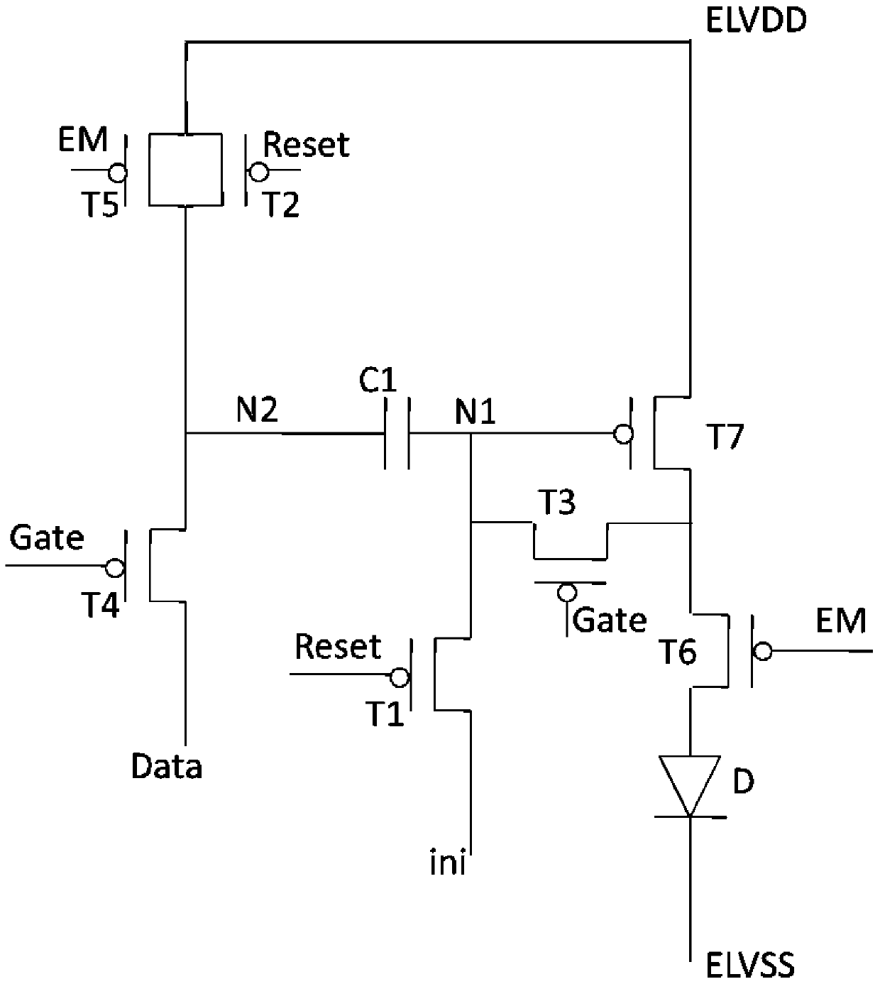
[0041] The specific implementation manners of the present invention will be further described in detail below in conjunction with the accompanying drawings and embodiments. The following examples are used to illustrate the present invention, but are not intended to limit the scope of the present invention.

[0042] It should be noted that the gate of each transistor defined in the embodiment of the present invention is one end that controls the opening of the transistor, and the source and drain are the two ends of the transistor except the gate. Here, the source and drain are only for convenience of description The connection relationship of the transistors does not limit the direction of the current. Those skilled in the art can clearly know the working principle and state of the transistors according to the type of the transistors and the signal connection mode.

[0043] Such as figure 1 As shown, the pixel driving circuit of the embodiment of the present invention includes:...


PUM


Abstract

The invention relates to the field of display technology and discloses a pixel driving circuit, which includes: a data line, a gate line, a first power line, a second power line, a light-emitting device, a driving transistor, a storage capacitor, a reset unit, and a data writing unit. Compensation unit and lighting control unit. The invention also discloses a driving method, array substrate and display device. The pixel driving circuit of the present invention can compensate and eliminate display unevenness caused by threshold voltage differences of driving transistors.

Description

technical field [0001] The present invention relates to the field of display technology, in particular to a pixel driving circuit, a driving method, an array substrate and a display device. Background technique [0002] Organic Light-Emitting Diode (OLED), as a current-mode light-emitting device, has been increasingly used in high-performance active-matrix light-emitting OLEDs. Traditional passive matrix organic electroluminescent display tubes (Passive Matrix OLED) require a shorter driving time of a single pixel as the display size increases, thus requiring an increase in transient current and power consumption. At the same time, the application of a large current will cause an excessive voltage drop on the ITO metal oxide line, and make the working voltage of the OLED too high, thereby reducing its efficiency. However, an active matrix organic electroluminescent display tube (Active Matrix OLED, AMOLED) scans input OLED current row by row through switching transistors, w...

Claims


Application Information

Patent Timeline
Patent Type & Authority Patents(China)
IPC IPC(8): G09G3/3233
CPCG09G2300/0861G09G2310/0251G09G2320/043G09G3/3233G09G2300/0819G09G3/3258G09G2320/0233G09G2320/0257G09G2320/045G09G2320/0626
Inventor 孙亮王颖孙拓马占洁殷新社张林涛皇甫鲁江
Owner BOE TECH GRP CO LTD
Why Eureka
Try Eureka