Pixel driving circuit, driving method, array substrate and display device

A pixel driving circuit and driving transistor technology are applied in the fields of pixel driving circuits, driving methods, array substrates and display devices to achieve the effects of improving driving effect, eliminating non-uniformity and improving quality

Active Publication Date: 2017-05-31
BOE TECH GRP CO LTD
View PDF5 Cites 1 Cited by
  • Summary
  • Abstract
  • Description
  • Claims
  • Application Information

AI Technical Summary

Problems solved by technology

[0009] The technical problem to be solved by the present invention is: how to realize an AMOLED pixel drive circuit capable of compensating and eliminating the display unevenness caused by the difference in the threshold voltage of the drive transistor

Method used


Image

  • Pixel driving circuit, driving method, array substrate and display device
  • Pixel driving circuit, driving method, array substrate and display device
  • Pixel driving circuit, driving method, array substrate and display device

Examples


Embodiment 1

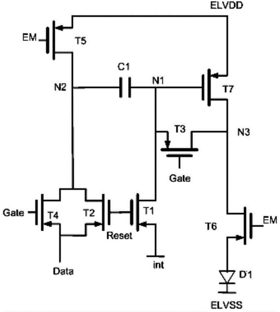
[0046] Such as figure 1 As shown, the pixel driving circuit of the present invention includes: data line Data, gate line Gate, first power line ELVDD, second power line ELVSS, light emitting device D1, driving transistor T7, storage capacitor C1, reset unit, data writing unit, compensation unit and lighting control unit. The light-emitting device D1 can be an organic light-emitting diode; the data line Data is used to provide a data voltage; the gate line Gate is used to provide a scanning voltage; the first power supply line ELVDD is used to provide a first power supply voltage, and the second power supply Line ELVSS is used to provide the second power supply voltage.

[0047] The reset unit is used to reset the voltage across the storage capacitor C1 to a predetermined voltage.

[0048] The data writing unit is connected to the gate line Gate, the data line Data and the first end (N1 point) of the storage capacitor C1, and is used for writing information including the data...

Embodiment 2

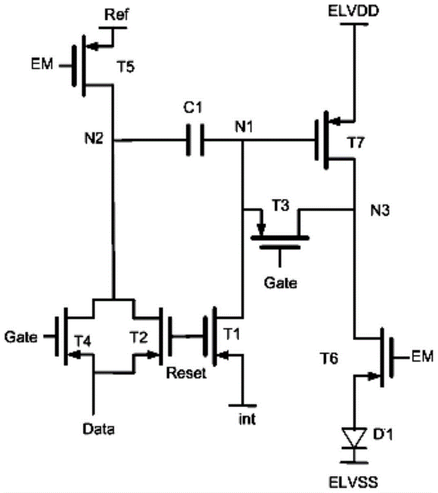
[0065] In Embodiment 1, T5 is connected to the first power line ELVDD, and the current resistance voltage drop (IRdrop) on the first power line ELVDD causes the voltage V dd Therefore, when T5 charges the second terminal (N2 point) of C1, the gate voltages of the driving transistors of different pixel units will be different, V dd The effect of the drop on the current will cause the problem of uneven brightness of different pixels.

[0066] Therefore, the pixel driving circuit of this embodiment further includes a compensation signal line for compensating the variation of the first power supply voltage.

[0067] Specifically as image 3 As shown, the structure of the pixel driving circuit in this embodiment is basically the same as that in Embodiment 1, the difference is that the pixel driving circuit in this embodiment further includes a compensation signal line Ref, and the source of the fifth transistor T5 of the light emission control unit is connected to this Compensation...

Embodiment 3

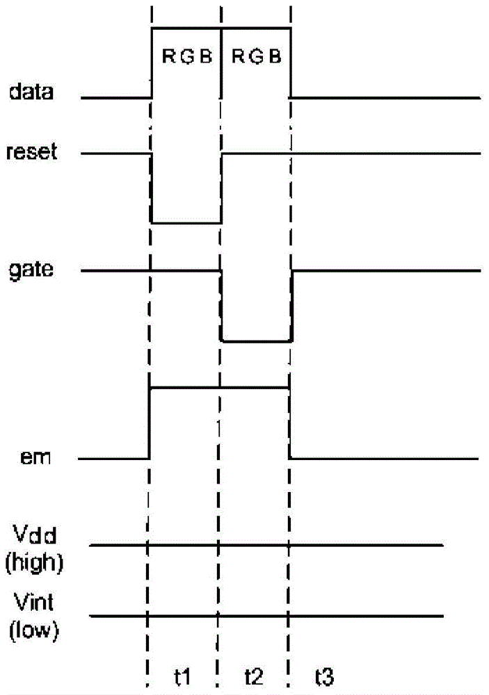
[0075] The present invention provides a pixel driving method for the pixel driving circuit of the above-mentioned embodiment 1 or embodiment 2, including the following process:

[0076] In the reset phase, the reset unit resets the voltage across the storage capacitor to a predetermined voltage;

[0077] In the data voltage writing phase, the data writing unit writes the data voltage to the second end of the storage capacitor, and the compensation unit writes information including the threshold voltage of the driving transistor and the first power supply voltage information to the first end of the storage capacitor ;

[0078] In the light emitting stage, the storage capacitor transfers the information including the data voltage to the gate of the driving transistor, and the driving transistor is controlled according to the information including the data voltage, the threshold voltage of the driving transistor and the first power supply voltage under the control of the light em...


PUM


Abstract

The present invention relates to the field of display technology, and discloses a pixel drive circuit, including: data lines, gate lines, first power lines, second power lines, light emitting devices, drive transistors, storage capacitors, reset units, data writing units, Compensation unit and lighting control unit. The invention also discloses a driving method, an array substrate and a display device. The pixel driving circuit of the present invention can compensate and eliminate display unevenness caused by the threshold voltage difference of driving transistors.

Description

technical field [0001] The present invention relates to the field of display technology, in particular to a pixel driving circuit, a driving method, an array substrate and a display device. Background technique [0002] Organic Light-Emitting Diode (OLED), as a current-mode light-emitting device, has been increasingly used in high-performance active-matrix light-emitting OLEDs. Traditional passive matrix organic electroluminescent display devices (Passive Matrix OLED) require shorter driving time of a single pixel as the display size increases, and thus need to increase transient current and increase power consumption. At the same time, the application of a large current will cause an excessive voltage drop on the ITO metal oxide line, and make the working voltage of the OLED too high, thereby reducing its efficiency. However, an active matrix organic electroluminescent display tube (Active Matrix OLED, AMOLED) scans input OLED current row by row through switching transisto...

Claims


Application Information

Patent Timeline
Patent Type & Authority Patents(China)
IPC IPC(8): G09G3/3233
CPCG09G3/3233G09G2300/0819G09G2300/0861G09G2310/0251G09G2310/0262G09G2320/0223G09G2320/043G09G2320/0233G09G3/2003G09G3/3225G09G2330/028
Inventor 孙亮王颖孙拓马占洁张林涛皇甫鲁江
Owner BOE TECH GRP CO LTD
Why Eureka
Try Eureka