Fingerprint collection device and manufacturing method thereof, fingerprint collection panel and display panel

A technology of fingerprint collection and production method, which is applied in the direction of acquiring/arranging fingerprints/palmprints, electric solid-state devices, semiconductor devices, etc., and can solve problems such as TFT operating current becomes smaller, threshold voltage becomes larger, and TFT switching characteristics are reduced

Active Publication Date: 2019-04-05
BOE TECH GRP CO LTD +1
View PDF6 Cites 0 Cited by
  • Summary
  • Abstract
  • Description
  • Claims
  • Application Information

AI Technical Summary

Problems solved by technology

However, doping, annealing and other processes are required to make photodiodes, which will reduce the switching characteristics of TFTs.
[0006] For example, the temperature used in the annealing process is generally above 650 degrees, and the TFT cannot withstand such a high temperature, which will change the electrical characteristics of the TFT, for example, the operating current of the TFT will be reduced, and the threshold voltage will be increased. Or the migration rate becomes smaller, etc.

Method used


Image

  • Fingerprint collection device and manufacturing method thereof, fingerprint collection panel and display panel
  • Fingerprint collection device and manufacturing method thereof, fingerprint collection panel and display panel
  • Fingerprint collection device and manufacturing method thereof, fingerprint collection panel and display panel

Examples


Embodiment Construction

[0031] The following will clearly and completely describe the technical solutions in the embodiments of the present invention with reference to the accompanying drawings in the embodiments of the present invention. Obviously, the described embodiments are only some, not all, embodiments of the present invention.

[0032] In addition, the terms "first" and "second" are used for descriptive purposes only, and cannot be understood as indicating or implying relative importance or implicitly specifying the quantity of indicated technical features. Thus, a feature defined as "first" and "second" may explicitly or implicitly include one or more of these features. In the description of the present invention, unless otherwise specified, "plurality" means two or more.

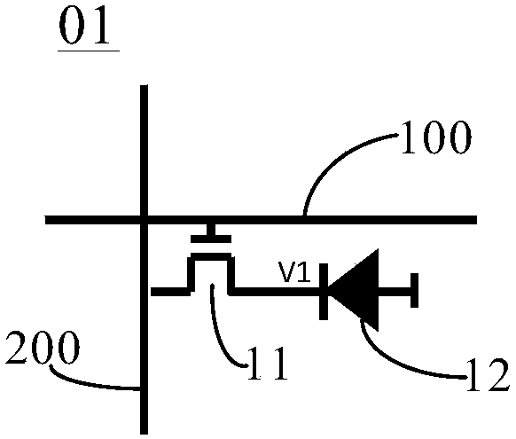
[0033] A fingerprint collection device provided by an embodiment of the present invention can be applied in the process of optical fingerprint collection. In order to more clearly explain the structure and implementation...


PUM


Abstract

Embodiments of the present invention provide a fingerprint collection device and a manufacturing method thereof, a fingerprint collection panel and a display panel, which relate to the field of display technology and can ensure the switching characteristics of TFTs when manufacturing the fingerprint collection device. The fingerprint collection device includes a TFT arranged on a substrate, and a photodiode connected to the drain of the TFT, the TFT includes a gate, an active layer, a source and the drain, further, the The fingerprint collection device further includes: a metal pattern disposed opposite to the gap between the source electrode and the drain electrode, and the metal pattern is disposed on a side of the active layer away from the base substrate. The array substrate can be applied in the process of fingerprint collection.

Description

technical field [0001] The invention relates to the field of display technology, in particular to a fingerprint collection device and a manufacturing method thereof, a fingerprint collection panel and a display panel. Background technique [0002] Photosensitive diodes can convert light signals of different light intensities into electrical signals. Therefore, in optical fingerprint collection technology, the photosensitive characteristics of photodiodes are usually used to collect the fingerprint information of the subject. [0003] Specifically, the fingerprint collection device can specifically include a TFT (Thin Film Transistor, thin film transistor) and a photodiode, wherein the cathode of the photodiode can be connected to the TFT, and the anode of the photodiode can be grounded, so that when the TFT is turned on, the photodiode is in the reverse bias state. [0004] When the finger presses the fingerprint collection device, the reflected light intensity of the valle...

Claims


Application Information

Patent Timeline
Patent Type & Authority Patents(China)
IPC IPC(8): H01L27/144G06K9/00
CPCH01L27/1443G06V40/1318
Inventor 刘英明董学薛海林陈小川王海生杨盛际丁小梁王鹏鹏赵卫杰李昌峰刘伟
Owner BOE TECH GRP CO LTD
Why Eureka
Try Eureka