Junction-bar gallium nitride-based high-electron-mobility transistor

A high electron mobility, gallium nitride based technology, applied in the field of junction strip gallium nitride based high electron mobility transistors, can solve the problem of insufficient withstand voltage capability, inability to exert device leakage current, and increase reverse withstand voltage gate Leakage current and other problems, to ensure the frequency characteristics and switching characteristics, avoid Miller capacitance effect, and improve the effect of breakdown voltage

Pending Publication Date: 2022-07-22
SOUTH CHINA UNIV OF TECH
View PDF0 Cites 0 Cited by
  • Summary
  • Abstract
  • Description
  • Claims
  • Application Information

AI Technical Summary

Problems solved by technology

For this reason, the present invention proposes a junction bar GaN-based high electron mobility transistor, which overcomes the insufficient withstand voltage capability of the GaN HEMT device, the inability to exert the critical high breakdown electric field of the GaN material, and the gate Schottky contact in the reverse direction. The problem of the leakage current of the lower device can increase the breakdown voltage of the device, increase the reverse withstand voltage of the device and reduce the gate leakage current of the device in the off state

Method used


Image

  • Junction-bar gallium nitride-based high-electron-mobility transistor
  • Junction-bar gallium nitride-based high-electron-mobility transistor
  • Junction-bar gallium nitride-based high-electron-mobility transistor

Examples


Embodiment 1

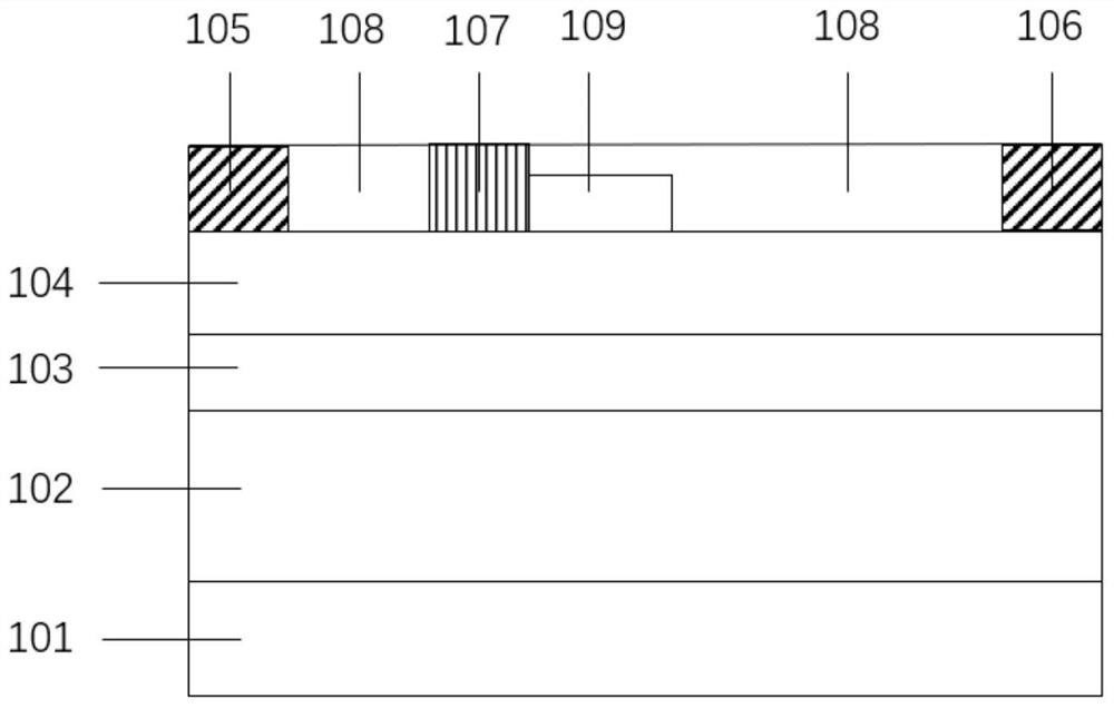
[0037] This embodiment provides a junction stripe GaN-based high electron mobility transistor, the schematic diagram of which is as follows: figure 1As shown, its structure includes a substrate 101, a buffer layer 102, a GaN channel layer 103, an AlGaN barrier layer 104, a source electrode 105, a gate electrode 106, a drain electrode 107, a passivation layer 108, and a P-type doped AlGaN strip 109 ; The substrate 101, the buffer layer 102, the GaN channel layer 103, and the AlGaN barrier layer 104 are stacked sequentially from bottom to top; the source electrode 105, the gate electrode 106, and the drain electrode 107 are respectively arranged on the AlGaN barrier The upper surface of the layer 104; the source electrode 105 and the drain electrode 107 both form ohmic contact with the upper surface of the AlGaN barrier layer 104, and the gate 106 and the upper surface of the AlGaN barrier layer 104 form a Schottky contact contact; the P-type doped AlGaN strips 109 are located o...

Embodiment 2

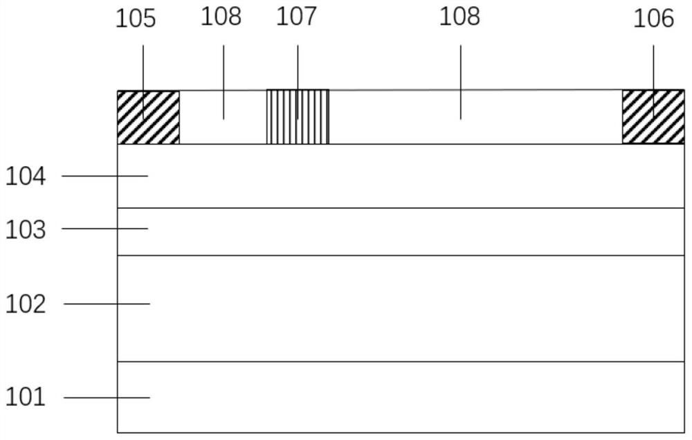
[0048] like Figure 5 As shown, this embodiment provides a junction stripe GaN-based high electron mobility transistor, the difference from Embodiment 1 is the unintentional doping of P-type doped AlGaN strips 109 between the gate 106 and the drain 107 Three PN junction strips are grown on the upper surface of the hetero AlGaN barrier layer 104, and the three P-type doped AlGaN strips 109 and the unintentionally doped AlGaN barrier layer 104 form multiple PN junction strips, and the total length of the multiple junction strips is The distance between the gate 106 and the drain 107 is not exceeded.

Embodiment 3

[0050] like Image 6 As shown, this embodiment provides a junction stripe GaN-based high electron mobility transistor. The difference from Embodiment 1 is that the P-type doped AlGaN stripe 109 is partially embedded between the gate 106 and the drain 107. In the doped AlGaN barrier layer 104, the depth of the unintentionally doped AlGaN barrier layer 104 between the gate 106 and the drain 107 embedded by the P-type doped AlGaN strips 109 is smaller than that of the P type doped AlGaN strip 109 height.


PUM

PropertyMeasurementUnit
Doping concentrationaaaaaaaaaa

Abstract

The invention provides a junction strip gallium nitride-based high electron mobility transistor. The structure of the transistor comprises a substrate, a buffer layer, a GaN channel layer, an AlGaN barrier layer, a source electrode, a grid electrode, a drain electrode, a passivation layer and at least one P-type doped AlGaN strip. The P-type doped AlGaN strip grows on the upper surface of the unintentionally doped AlGaN barrier layer between the grid electrode and the drain electrode, the longitudinally formed PN junction strip bears a part of voltage between the grid electrode and the drain electrode in the off-state of the device, the strong electric field peak value of the side, close to the drain electrode, of the grid electrode is reduced, the electric field between the grid electrode and the drain electrode is redistributed, and the device performance is improved. And the breakdown voltage of the device is effectively improved.

Description

technical field [0001] The invention belongs to the technical field of semiconductor devices, and in particular relates to a junction stripe gallium nitride-based high electron mobility transistor. Background technique [0002] With the further development of microwave radio frequency technology, the existing Si-based and GaAs-based power devices can no longer meet the requirements of high temperature, high withstand voltage, radiation resistance, high power, high efficiency, ultra-wide bandwidth and other working conditions. Performance requirements, in order to meet the development needs of future micro-power devices, since the 1990s, the research focus of microwave power devices began to shift to wide-bandgap semiconductor material devices. [0003] The third-generation semiconductor gallium nitride has the characteristics of large band gap, high breakdown voltage, and significant polarization effect. Therefore, GaN-based high electron mobility transistor devices represen...

Claims


Application Information

Patent Timeline
IPC IPC(8): H01L29/06H01L29/20H01L29/778
CPCH01L29/0615H01L29/2003H01L29/778
Inventor 李国强罗玲邢志恒吴能滔李善杰
Owner SOUTH CHINA UNIV OF TECH
Why Eureka
Try Eureka