Array substrate and its preparation method and display device

A technology for array substrates and display devices, which is applied in the field of array substrates and its preparation, and can solve problems such as thin film transistors that need to be further developed

Active Publication Date: 2020-11-06
BOE TECH GRP CO LTD
View PDF4 Cites 0 Cited by
  • Summary
  • Abstract
  • Description
  • Claims
  • Application Information

AI Technical Summary

Problems solved by technology

But the increase of the length value limits the further improvement of the resolution
[0004] Therefore, research on thin film transistors still needs to be in-depth

Method used


Image

  • Array substrate and its preparation method and display device
  • Array substrate and its preparation method and display device
  • Array substrate and its preparation method and display device

Examples


Embodiment Construction

[0021] Embodiments of the present invention are described in detail below. The embodiments described below are exemplary only for explaining the present invention and should not be construed as limiting the present invention. If no specific technique or condition is indicated in the examples, it shall be carried out according to the technique or condition described in the literature in this field or according to the product specification. The reagents or instruments used were not indicated by the manufacturer, and they were all commercially available conventional products.

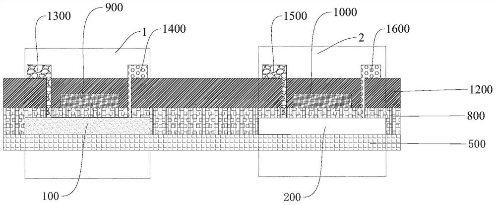
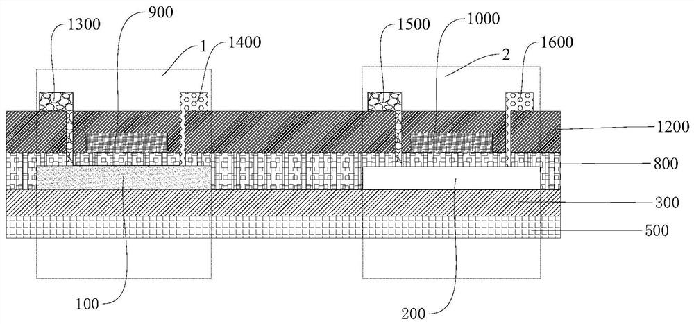
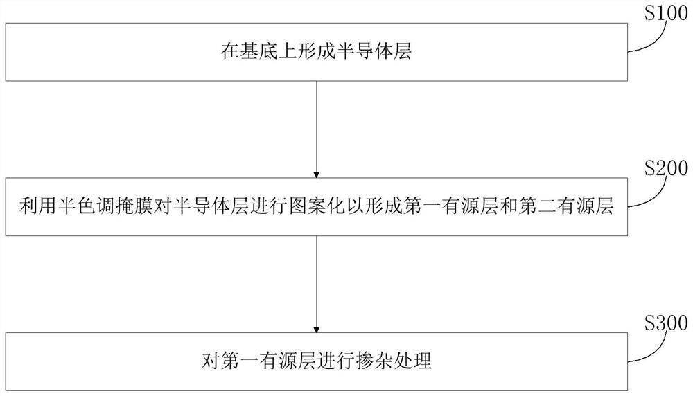
[0022] In one aspect of the present invention, the present invention provides an array substrate. According to an embodiment of the present invention, refer to figure 1 , the array substrate includes a switching thin film transistor 1 and a driving thin film transistor 2, wherein the first active layer 100 of the switching thin film transistor 1 is formed of a doped semiconductor material, and the second...


PUM

PropertyMeasurementUnit
thicknessaaaaaaaaaa

Abstract

The invention provides an array substrate, a preparation method thereof and a display device. The array substrate comprises a switch thin film transistor and a drive thin film transistor. A first active layer of the switch thin film transistor is formed by a doped semiconductor material. A second active layer of the drive thin film transistor is formed by a non-doped semiconductor material. According to the array substrate, the switching property of the switch transistor can be ensured, the carrier mobility of the switch thin film transistor is improved and the Vth offset is reduced; and moreover, on the premise of ensuring that the drive thin film transistor has ideal carrier mobility, the length of the active layer of the drive thin film transistor is reduced, and a high-resolution design demand is realized.

Description

technical field [0001] The present invention relates to the field of display technology, in particular, to an array substrate and a preparation method thereof. Background technique [0002] With the development of TFT-LCD technology, high carrier mobility, low power consumption, and high resolution have become the focus of everyone's attention. [0003] In the field of flat panel display technology, Low Temperature Poly-silicon Thin Film Transistor (LTPS TFT for short) has the advantages of high response speed, high aperture ratio, and high brightness, and has become the fastest growing flat panel display market today. technology. And it can also be used in flexible displays and organic light-emitting diode displays, known as next-generation display technology. The active layer of the low-temperature polysilicon thin film transistor is low-temperature polysilicon (p-Si), which needs to be ion-doped to increase its carrier mobility, such as B 3+ , to improve the switching ...

Claims


Application Information

Patent Timeline
Patent Type & Authority Patents(China)
IPC IPC(8): H01L27/12H01L29/786H01L21/77
CPCH01L27/1222H01L27/127H01L27/1288H01L29/78675
Inventor 王利忠杨维邸云萍周天民
Owner BOE TECH GRP CO LTD
Why Eureka
Try Eureka