

Semiconductor device
a technology of semiconductors and devices, applied in the direction of semiconductor devices, basic electric elements, electrical equipment, etc., can solve the problems of further suppressing on resistance and further reducing channel resistance, and achieve the effect of reducing channel resistan
- Summary
- Abstract
- Description
- Claims
- Application Information
AI Technical Summary
Benefits of technology
Problems solved by technology
Method used
Image

Examples
first embodiment
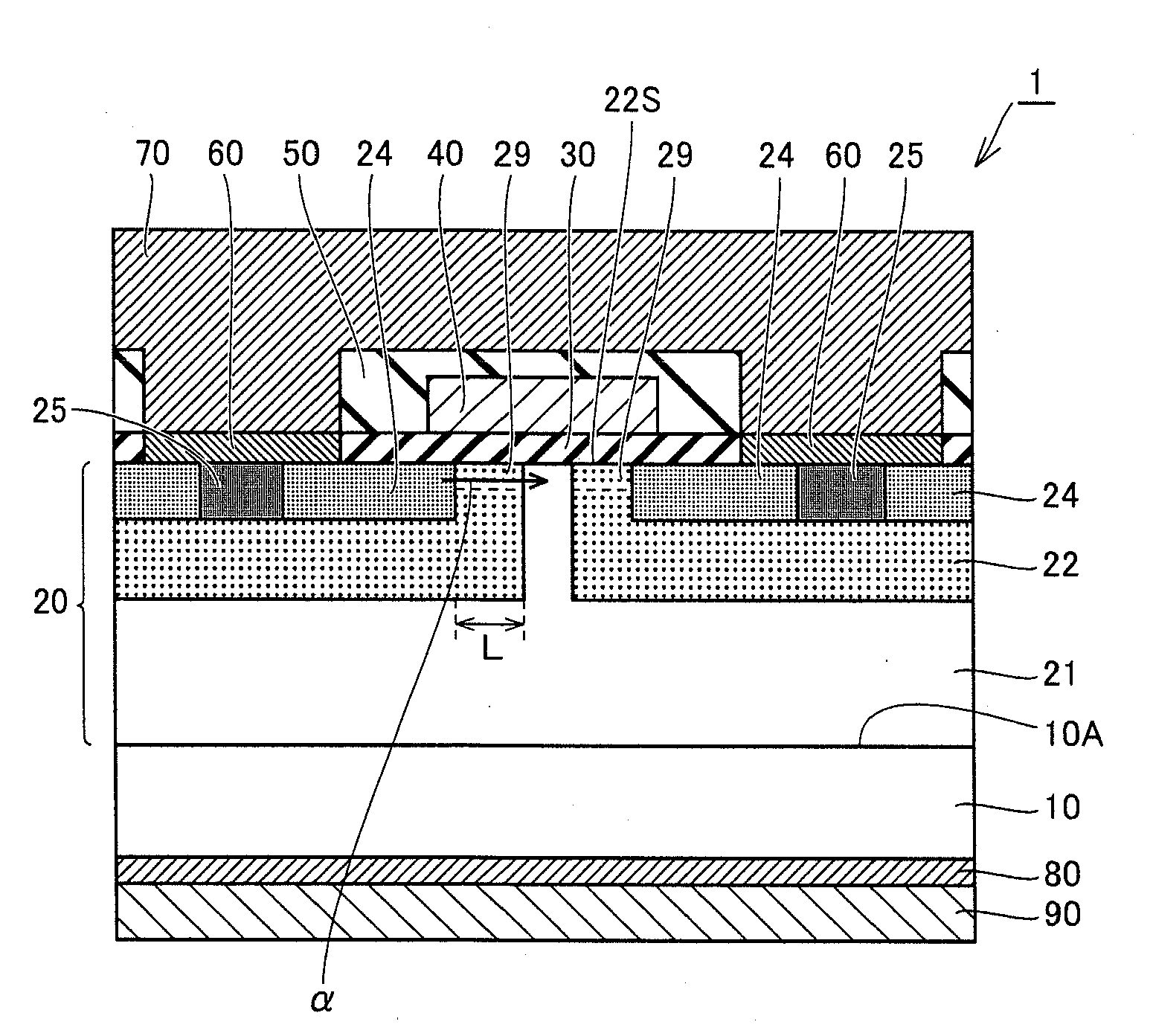
[0045]First, a first embodiment, which is one embodiment of the present invention, will be described below with reference to FIG. 1. A MOSFET 1, which is a semiconductor device of the first embodiment, includes a silicon carbide substrate 10 and an active layer 20 disposed on one main surface 10A of silicon carbide substrate 10. Active layer 20 is an epitaxial growth layer made of silicon carbide.
[0046]Silicon carbide substrate 10 is made of single-crystal silicon carbide, contains an impurity (n type impurity) such as nitrogen or phosphorus, and therefore has n type conductivity (first conductivity type). Active layer 20 includes a drift layer 21, p type body regions 22, n+ source regions 24, and p+ contact regions 25.
[0047]Drift layer 21 is disposed on silicon carbide substrate 10, contains an n type impurity at a concentration lower than that in silicon carbide substrate 10, and therefore has n type conductivity. Each of p type body regions 22 is disposed to include a main surfac...
second embodiment
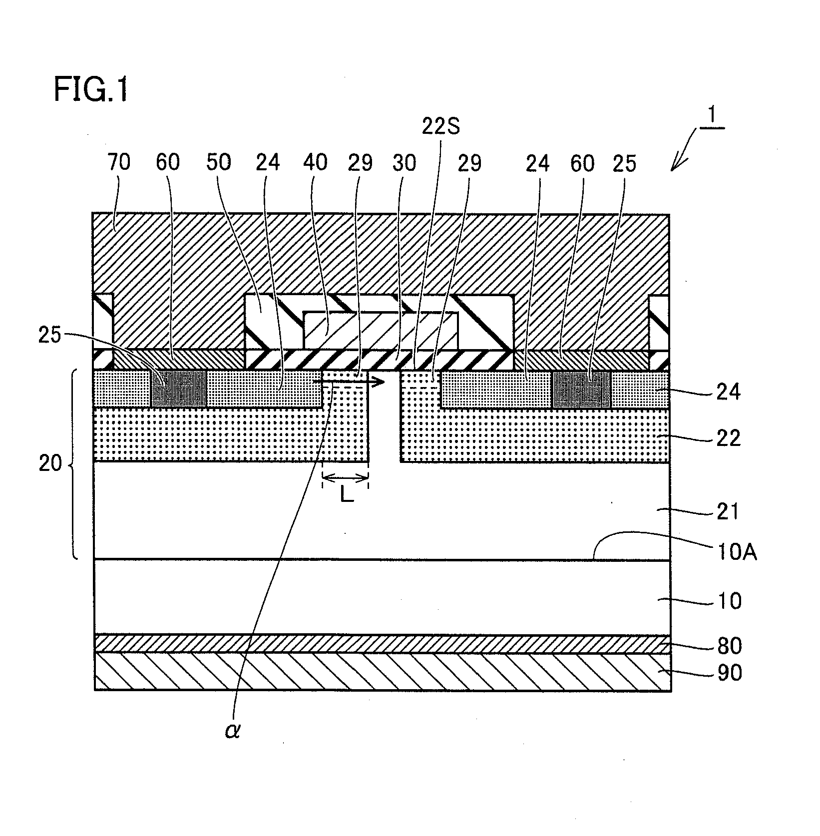
[0070]The following describes another embodiment of the present invention, i.e., a second embodiment. Referring to FIG. 10, a MOSFET 1, which is a semiconductor device in the second embodiment, has basically the same structure and provides basically the same effects as those of MOSFET 1 in the first embodiment. However, MOSFET 1 of the second embodiment is different from that of the first embodiment in terms of the configuration of each of p type body regions 22, in particular, the configuration of channel region 29.
[0071]Referring to FIG. 10, in MOSFET 1 of the second embodiment, each of p type body regions 22 includes: a high concentration region 22A containing acceptors at a high concentration; and a low concentration region 22B disposed to surround high concentration region 22A and containing acceptors at a concentration lower than that of high concentration region 22A. Further, gate oxide film 30 extends to make contact with n+ source regions 24, high concentration regions 22A,...
PUM
 Abstract
Description
Claims
Application Information