Semiconductor device

Active Publication Date: 2015-12-31
MITSUBISHI ELECTRIC CORP
View PDF5 Cites 11 Cited by
  • Summary
  • Abstract
  • Description
  • Claims
  • Application Information

AI Technical Summary

Benefits of technology

[0010]In the semiconductor device according to the present invention, the channel resistance of the channel formed in the first well region has the temperature characteristic that the channel resistance increases with increasing temperature and the channel resistance of the channel formed in the second well region

Problems solved by technology

Unfortunately, currently used SiC-MOSFETs have an ON resistanc

Method used


Image

  • Semiconductor device
  • Semiconductor device
  • Semiconductor device

Examples


embodiment 1

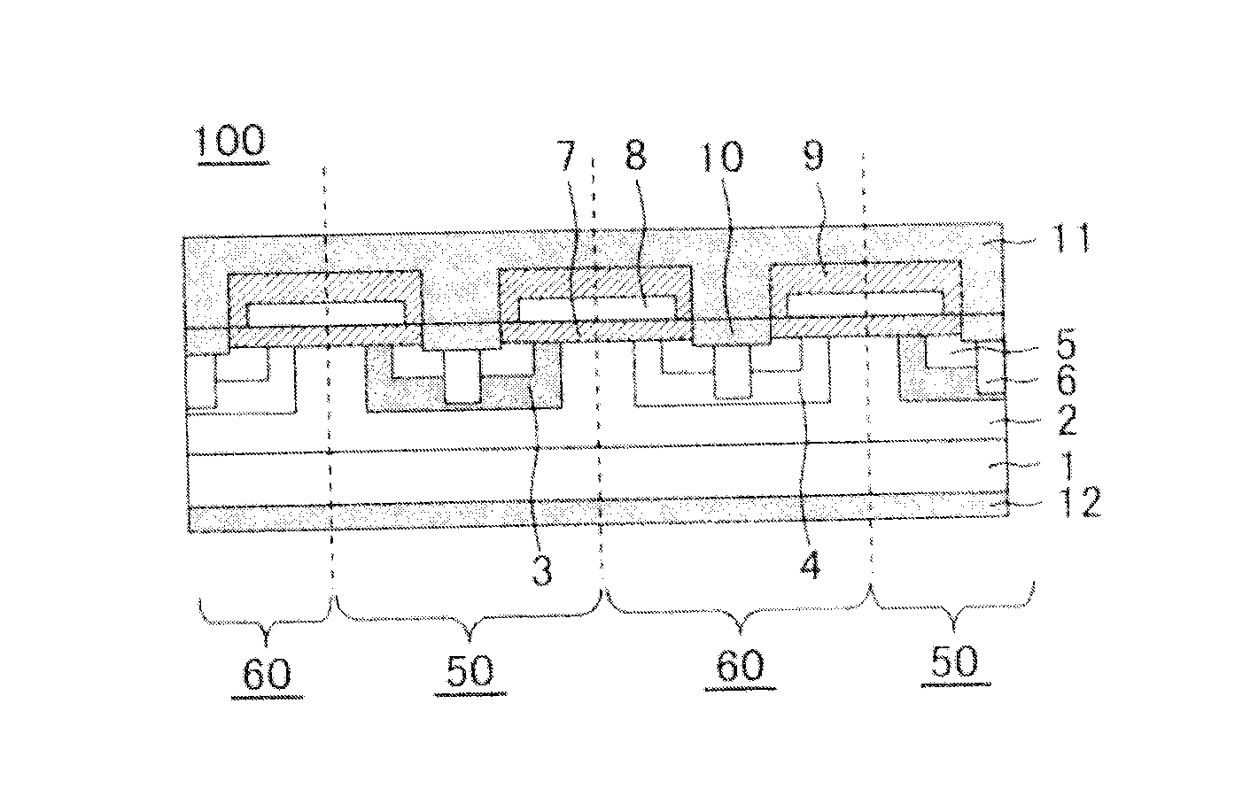
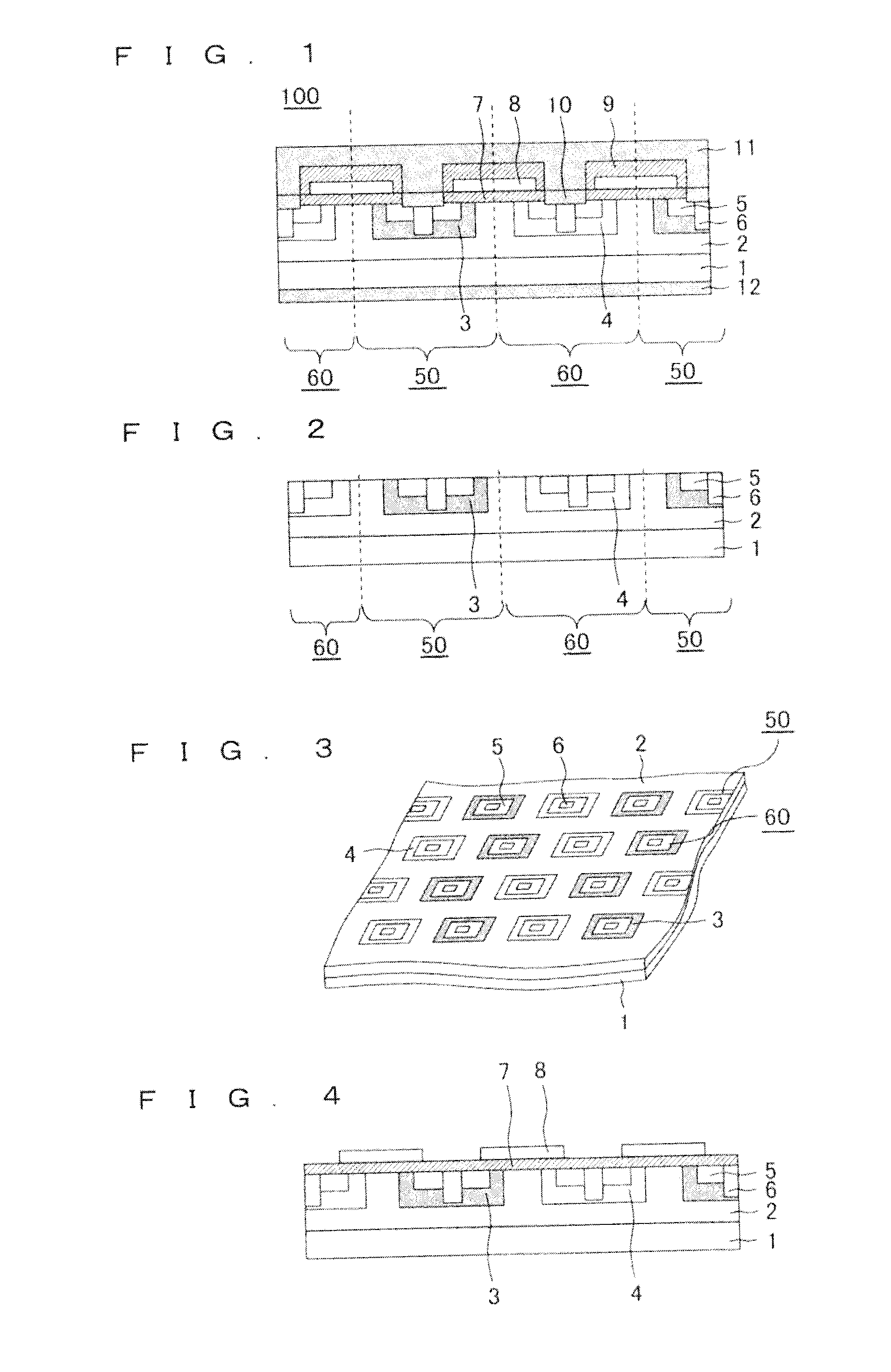
[0024]Firstly, a configuration of a semiconductor device according to an embodiment 1 of the present invention is described. FIG. 1 is a cross-sectional view of a part of the semiconductor device according to the embodiment 1 of the present invention. An n-type MOSFET is described as an example of the semiconductor device according to the present embodiment. Alternatively, the semiconductor device may be a p-type MOSFET or another insulated gate semiconductor device.

[0025]An effective acceptor density hereinafter refers to a density obtained by deducting the density of n-type impurities from the density of p-type impurities in a predetermined area. An effective acceptor concentration hereinafter refers to a concentration obtained by deducting the concentration of n-type impurities from the concentration of p-type impurities in a predetermined area. The effective acceptor density and the effective acceptor concentration are used to explain the n-type semiconductor device in the prese...

embodiment 2

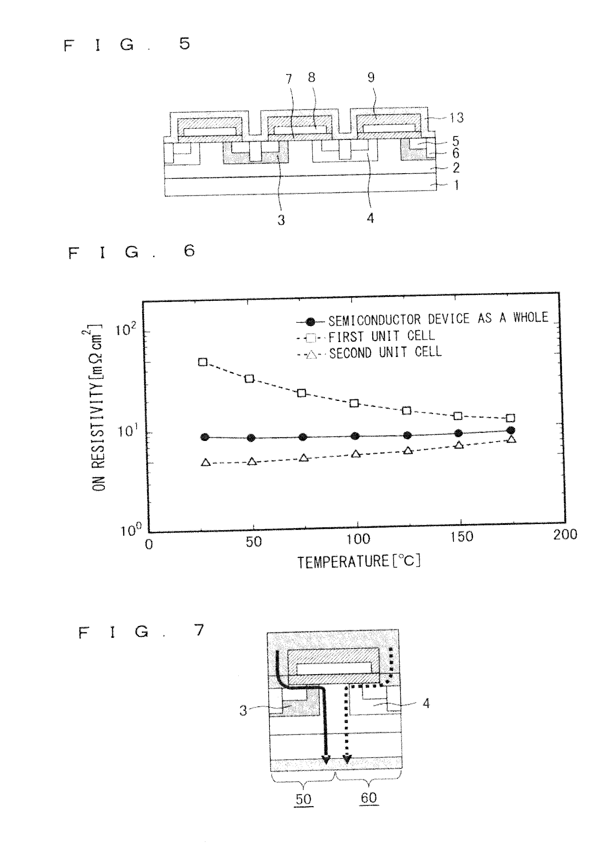
[0068]As described above, in the embodiment 1, the impurity concentration in the well region is adjusted to change the temperature characteristic of each unit cell. The present invention should not be limited to the above. As an embodiment 2, the following describes the semiconductor device in which the interface state density at the interface between the well region and the gate oxide film is adjusted to change the temperature characteristic of each unit cell.

[0069]The following describes an aspect different from the embodiment 1 of the present invention, in other words, the adjustment of the interface state density aimed to change the temperature characteristic of each unit cell, and the description of the same or corresponding aspect is omitted.

[0070]In the embodiment 1, the first and the second well regions 3 and 4 have different p-type impurity concentrations, so that the channel resistance has different temperature characteristics being positive and negative in different unit ...

embodiment 3

[0085]In the embodiments 1 and 2, a plurality of kinds of well regions are formed such that the channel resistance has different temperature characteristics in different unit cells. In the present embodiment, the well region is designed such that, out of the channels on a plurality of sides of each individual unit cell having a polygonal shape, the channels on some sides have the channel resistance value in the positive temperature characteristic and the channels on the other sides have the channel resistance in the negative temperature characteristic. This alleviates the temperature dependence of the ON resistance in each individual unit cell.

[0086]The following describes the aspect different from the embodiment 1 of the present invention, in other words, the adjustment of the dopant concentrations aimed to change the temperature characteristics of channels on a plurality of sides of each unit cell, and the description of the same or corresponding aspect is omitted.

[0087]A configur...


PUM


Abstract

A semiconductor device capable of reducing ON-resistance changes with temperature, including a semiconductor substrate of a first conductivity type, a drift layer of the first conductivity type formed on the semiconductor substrate, a first well region of a second conductivity type formed in the front surface of the drift layer, a second well region of the second conductivity type formed in the front surface of the drift layer, and a gate structure that is formed on the front surface of the drift layer and forms a channel in the first well region and a channel in the second well region. A channel resistance of the channel formed in the first well region has a temperature characteristic that the channel resistance decreases with increasing temperature and a channel resistance of the channel formed in the second well region has a temperature characteristic that the channel resistance increases with increasing temperature.

Description

TECHNICAL FIELD[0001]The present invention relates to a semiconductor device, and more particularly, to an insulated gate semiconductor device.BACKGROUND ART[0002]Switching elements such as insulated gate bipolar transistors (IGBTs) or metal oxide semiconductor field effect transistors (MOSFETs) made of silicon (Si) have been customarily included in power electronics equipment. In recent years, switching elements made of silicon carbide (SiC) having physical properties superior to those of Si have been actively developed.[0003]The withstand voltage of MOSFETs depends on the thickness of the drift layer. SiC has a breakdown electric field higher than that of Si, and thus, the drift layer of a MOSFET made of SiC having a withstand voltage equal to that of a MOSFET made of Si can be thinner than the drift layer of the MOSFET made of Si. The ON resistance of the MOSFET is composed of, for example, channel resistance, JFET resistance, drift resistance, and substrate resistance. The SiC-M...

Claims


Application Information

Patent Timeline
IPC IPC(8): H01L29/16H01L29/78
CPCH01L29/78H01L29/7395H01L29/7397H01L21/049H01L29/34H01L29/66068H01L29/7802H01L29/7813H01L29/0696H01L29/1033H01L29/1095H01L29/1608
Inventor FURUHASHI, MASAYUKIOKABE, HIROAKIWATANABE, TOMOKATSUIMAIZUMI, MASAYUKI
Owner MITSUBISHI ELECTRIC CORP
Why Eureka
Try Eureka