
Method for manufacturing semiconductor device having super junction construction

a manufacturing method and semiconductor technology, applied in the direction of thermoelectric device junction materials, semiconductor devices, electrical apparatus, etc., can solve the problem of lower and achieve the effect of preventing floating, small state resistance, and low manufacturing cost of semiconductor devices

Inactive Publication Date: 2006-06-29
DENSO CORP
View PDF8 Cites 16 Cited by
  • Summary
  • Abstract
  • Description
  • Claims
  • Application Information

AI Technical Summary

Benefits of technology

The present invention provides a semiconductor device with low on state resistance without increasing manufacturing costs. This is achieved by reducing the impurity concentration of the drift region near the trench gate electrode and preventing potential instability. The device includes a body region, a drift region, and a trench gate electrode. The drift region has two parts, with the first part having the same conductive type as the body region and extending in the same direction as the trench gate electrode. The second part has a different conductive type and is disposed between the first and third parts. The device also includes a semiconductor layer with lower impurity concentration than the drift region, which further reduces the on state resistance. The manufacturing method involves forming a plurality of trenches and insulation films in parallel, and embedding a gate electrode in each trench through an insulation film. The impurity concentration of the first part of the drift region is lower than that of the body region, and the potential of the first part is stable. The method also includes reducing the impurity concentration of the portion of the drift region near the trench gate electrode. Overall, the invention provides a semiconductor device with low on state resistance and stable potential without increasing manufacturing costs.

Problems solved by technology

Therefore, the manufacturing cost of the semiconductor device becomes lower.

Method used


Image

  • Method for manufacturing semiconductor device having super junction construction
  • Method for manufacturing semiconductor device having super junction construction
  • Method for manufacturing semiconductor device having super junction construction

Examples


first embodiment

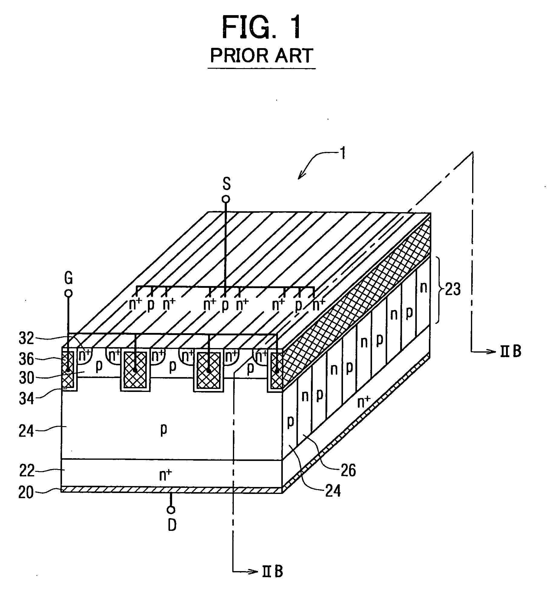
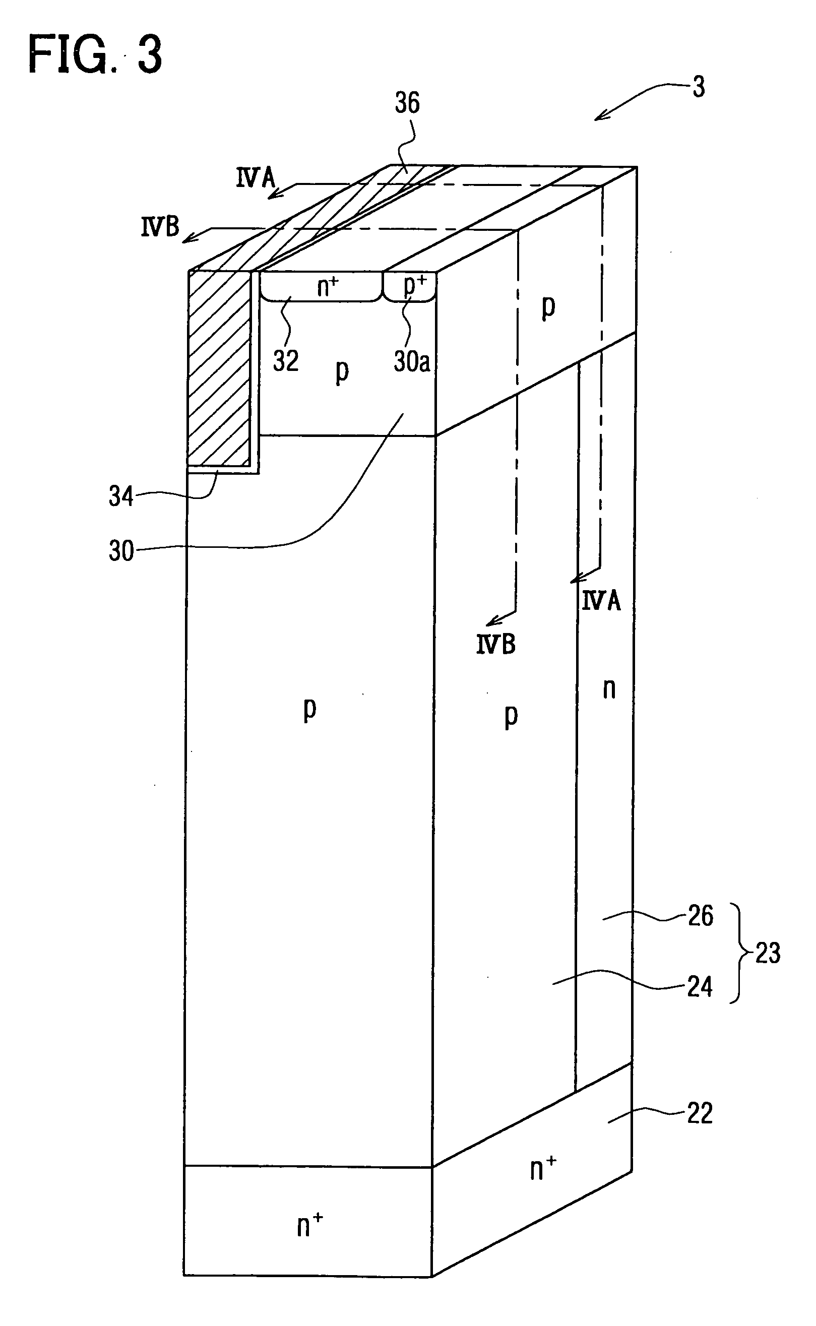
[0052] A semiconductor device 3 with a vertical type MOSFET having a trench gate electrode according to a first embodiment of the present invention is shown in FIG. 3. FIG. 3 shows a pair of a P type column 24 and an N type column 26 as a unit of an alternate layer (i.e., an alternation of strata). The semiconductor device 3 includes a source region 32, a body contact region 30a, a body region 30, a drift region 23, a drain region 22, a trench gate electrode 36 and a gate insulation layer 34. The source region 32 has N type conductivity. The body contact region 30a has P type conductivity. The body region 30 has the P type conductivity, and separates between the source region 32 and the drift region 23. The body contact region 30a contacts the body region 30. The drift region 23 includes the P type column (i.e., the first part) 24 and the N type column (i.e., the second part) 26. The p type column 24 extends between the body region 30 and the drain region 22. The N type column 26 ad...

second embodiment

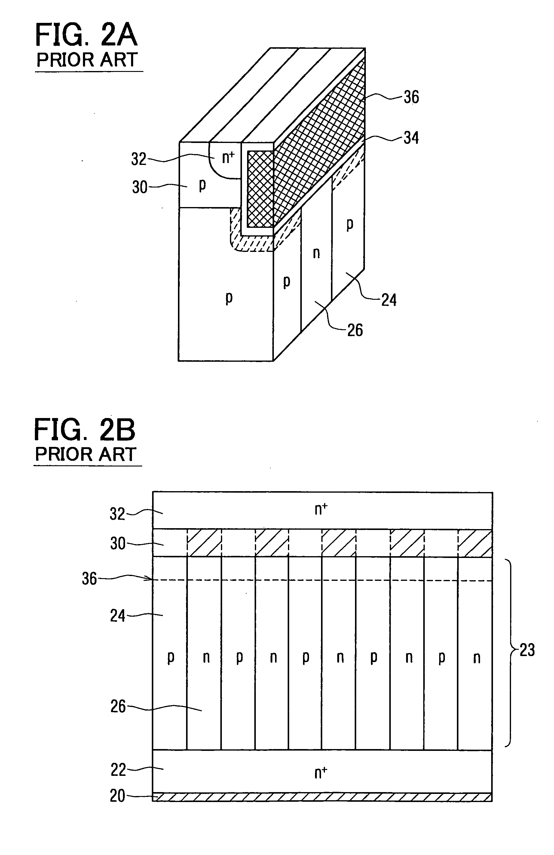
[0072]FIGS. 6A and 6B shows another semiconductor device 4 according to a second embodiment of the present invention. The semiconductor device 4 has the same construction as the semiconductor device 3 shown in FIG. 3. However, in the semiconductor device 4, the impurity concentration of the P type column 24 is equal to the impurity concentration of the P type body region 30.

[0073]FIG. 6A shows the current distribution of the P type column 24. FIG. 6B is an enlarged cross sectional view showing around the trench gate electrode 36. At this time, the bias voltage condition of the semiconductor device 4 is as follows. The source voltage (i.e., Vs) is zero Volts, the drain voltage (i.e., Vd) is 0.1 Volts, and the gate voltage (i.e., Vg) is 15 Volts.

[0074] As shown in FIG. 6B, the current flows from the N type column 26, and branches to flow the upside of the P type column 24 facing the bottom of the trench gate electrode 36. Further, the current also flows in the P type body region 30 ...

third embodiment

[0085] A semiconductor device 6 according to a third embodiment of the present invention is shown in FIG. 8. The device 6 has the vertical type MOSFET with the trench gate electrode. The semiconductor device 6 includes the source region 32, the body region 30, the drift region 23, the drain region 22, the trench gate electrode 36 and the gate insulation layer 34. The source region 32 has the N type conductivity. The body contact region 30a has the P type conductivity, and separates between the source region 32 and the drift region 23. The body contact region 30a contacts the P type body region 30. The impurity concentration of a part of the P type column 24 disposed on the P type body region side is equal to or smaller than that of the P type body region 30. The part of the P type column 24 represents as a P− type region 24a in FIG. 8. The impurity concentration of other part of the P type column 24 except for the P− type region 24a is equal to or larger than that of the P type body...


PUM


Abstract

A semiconductor device includes a body region, a drift region having a first part and a second part, and a trench gate electrode. The body region is disposed on the drift region. The first and second parts extend in an extending direction so that the second part is adjacent to the first part. The trench gate electrode penetrates the body region and reaches the drift region so that the trench gate electrode faces the body region and the drift region through an insulation layer. The trench gate electrode extends in a direction crossing with the extending direction of the first and second parts. The first part includes a portion near the trench gate electrode, which has an impurity concentration equal to or lower than that of the body region.

Description

CROSS REFERENCE TO RELATED APPLICATION [0001] This application is based on Japanese Patent Application No. 2003-179635 filed on Jun. 24, 2003, the disclosure of which is incorporated herein by reference. FIELD OF THE INVENTION [0002] The present invention relates to a semiconductor device having a super junction construction and a method for manufacturing the same. BACKGROUND OF THE INVENTION [0003] A vertical type MOSFET (i.e., metal-oxide semiconductor field effect transistor) having a trench gate electrode has low on-state resistance and high withstand voltage. Therefore, the vertical type MOSFET is suitably used for a switching device in power electronic equipment. When the on-state resistance and the withstand voltage are improved much more, a relationship between the on-state resistance and the withstand voltage shows a trade-off relationship. Specifically, when the on-state resistance is reduced, the withstand voltage decreases. When the withstand voltage is increased, the on...

Claims


Application Information

Patent Timeline
Patent Type & Authority Applications(United States)
IPC IPC(8): H01L29/08H01L35/24H01L21/336H01L29/06H01L29/10H01L29/78H10N10/856
CPCH01L29/0634H01L29/1095H01L29/7813
Inventor YAMAGUCHI, HITOSHISUZUKI, MIKIMASAHATTORI, YOSLHIYUKI
Owner DENSO CORP
Learn More