Level shifter for detecting grounded power-supply and level shifting method
a level shifter and power supply technology, applied in logic circuits, logic circuit coupling/interface arrangements, pulse techniques, etc., can solve the problems of additional static current consumption, large static consumption, and large static consumption
- Summary
- Abstract
- Description
- Claims
- Application Information
AI Technical Summary
Benefits of technology
Problems solved by technology
Method used
Image
Examples
embodiment 1
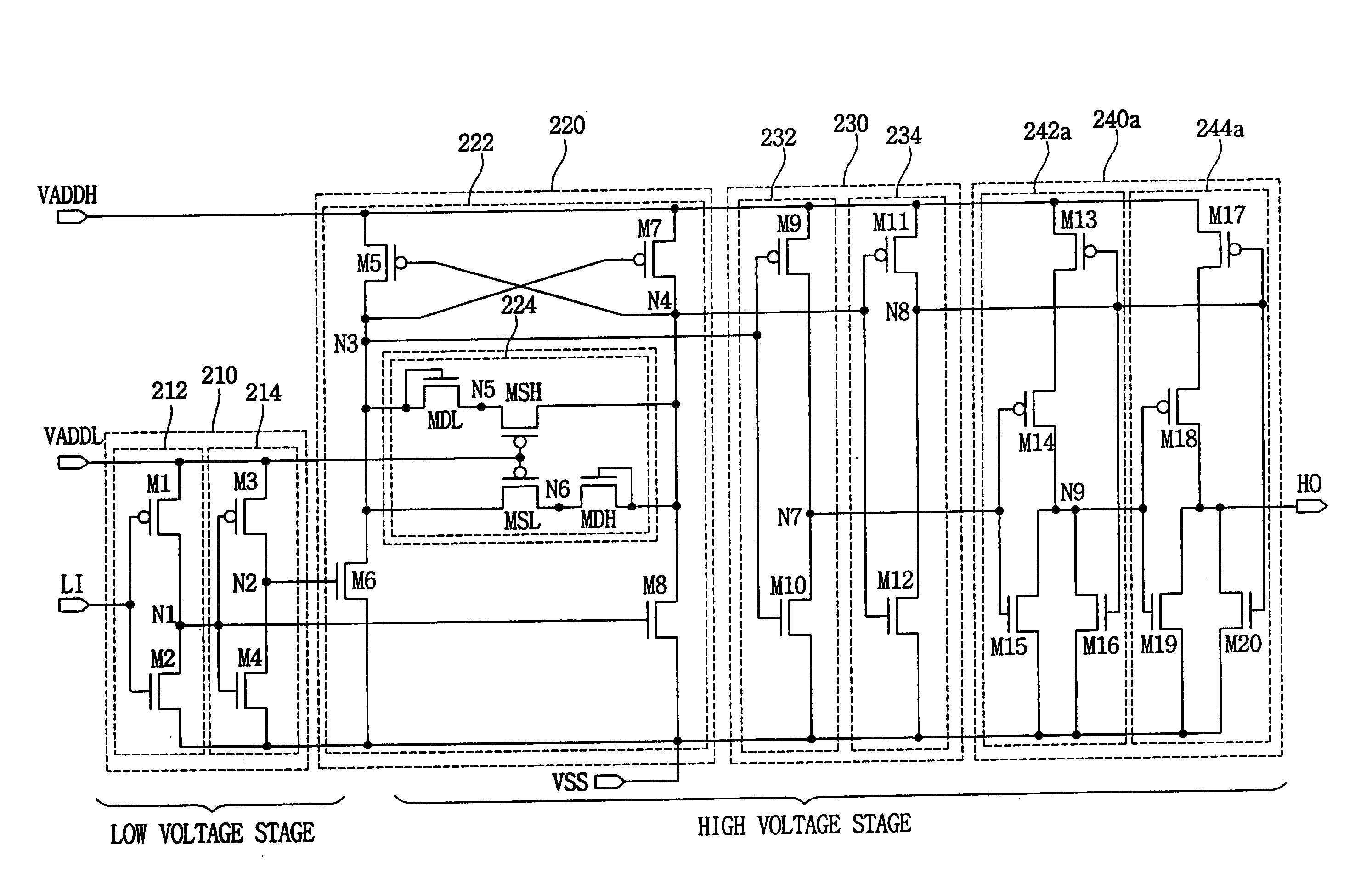
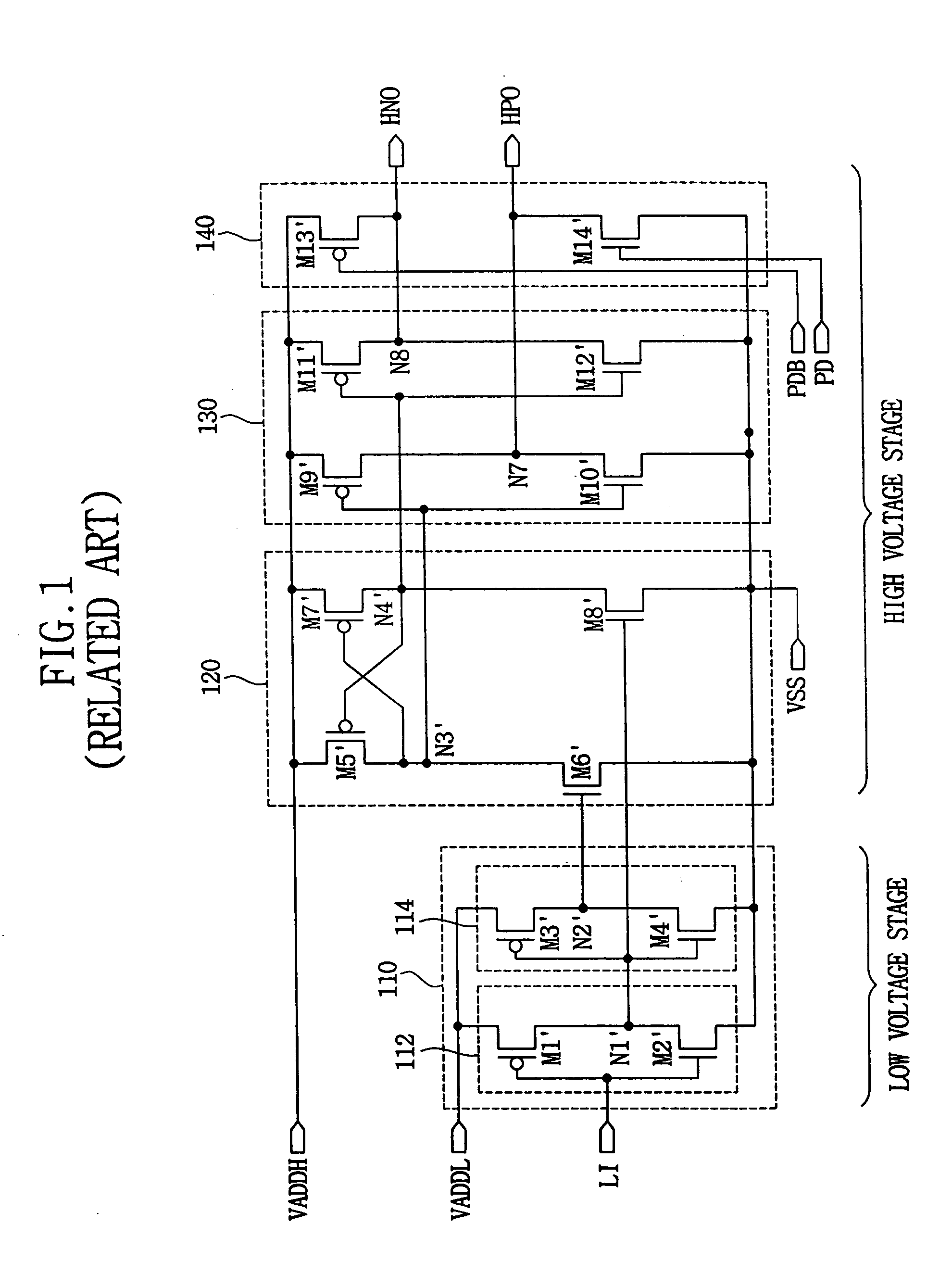
[0056]FIG. 3 is a circuit diagram of a low-to-high voltage level shifter of the FIG. 2 according to a first exemplary embodiment of the present invention.
[0057] Referring to FIG. 3, an input buffer 210 has a first inverter 212 and a second inverter 214. The first inverter 212 has a PMOS transistor M1 and an NMOS transistor M2. The second inverter 214 has a PMOS transistor M3 and an NMOS transistor M4.
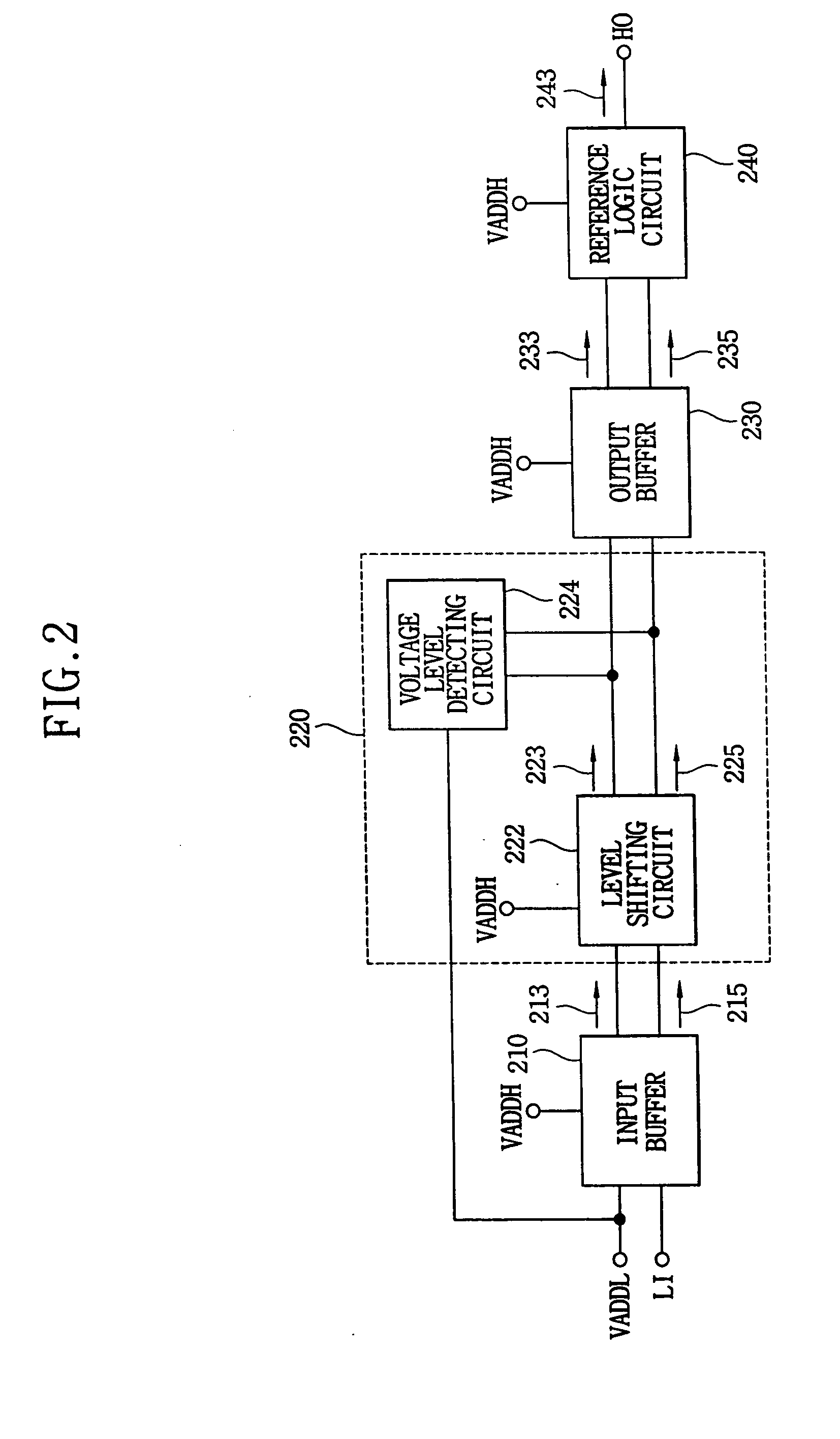
[0058] The input buffer 210 is activated by a first power voltage VADDL having a low-voltage level. The input buffer 210 receives a small range input signal LI via the first inverter 212, outputs a first small range signal 213 having the same phase with respect to the input signal LI via a node N2 and outputs a second small range signal 215 having a reversed phase with respect to the input signal LI via a node N1.
[0059] A voltage level shifting circuit 220 has a level shifting circuit 222 and a voltage level detecting circuit 224.
[0060] The level shifting circuit 222 is activated by...
embodiment 2
[0115]FIG. 5 is a circuit diagram of a low-to-high voltage level shifter of FIG. 2 according to a second exemplary embodiment of the present invention.
[0116] Referring to FIG. 5, the low-to-high level shifter according to the second exemplary embodiment of the present invention has a reference logic circuit 240b that has NAND GATEs instead of the NOR GATEs. That is, the reference logic circuit 240b is implemented by using two NAND GATEs instead of two NOR GATEs. When the first power voltage VADDL is below the given voltage level, the nodes N7 and N8 have the high-voltage logic level ‘LOW’ and the output signal HO has the high-voltage logic level ‘HIGH’.
[0117] Hereinafter, an input buffer 210, a level shifting circuit 222, a voltage level detecting circuit 224 and an output buffer 230 of the low-to-high level shifter according to the second exemplary embodiment of the present invention are the same as those of the low-to-high level shifter according to the first exemplary embodimen...
PUM
 Abstract
Description
Claims
Application Information


