Semiconductor device and manufacturing method thereof and power supply apparatus using the same

a technology of semiconductor devices and manufacturing methods, applied in the direction of semiconductor devices, electrical devices, transistors, etc., to achieve the effect of high performan

Inactive Publication Date: 2008-09-11
RENESAS ELECTRONICS CORP
View PDF16 Cites 19 Cited by
  • Summary
  • Abstract
  • Description
  • Claims
  • Application Information

AI Technical Summary

Benefits of technology

[0006]The present inventors have found that the following problems about achievement of the high-voltage power transistor

Problems solved by technology

The present inventors have found that the following problems about achievement of the high-voltage power transistor acc

Method used


Image

  • Semiconductor device and manufacturing method thereof and power supply apparatus using the same
  • Semiconductor device and manufacturing method thereof and power supply apparatus using the same
  • Semiconductor device and manufacturing method thereof and power supply apparatus using the same

Examples


first embodiment

[0042]In a first embodiment, a trench-gate type field-effect transistor with a low channel resistance will be exemplified.

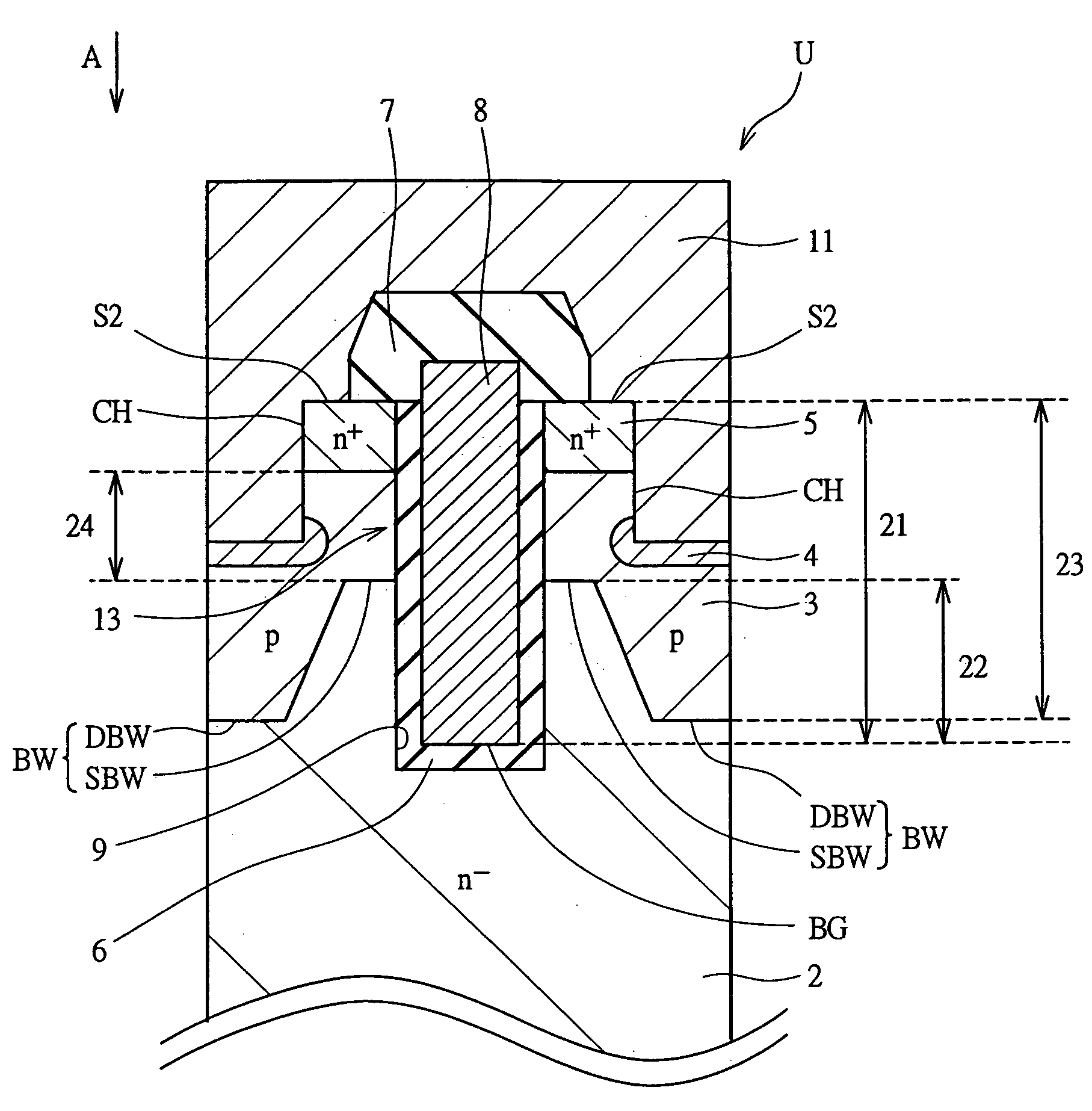
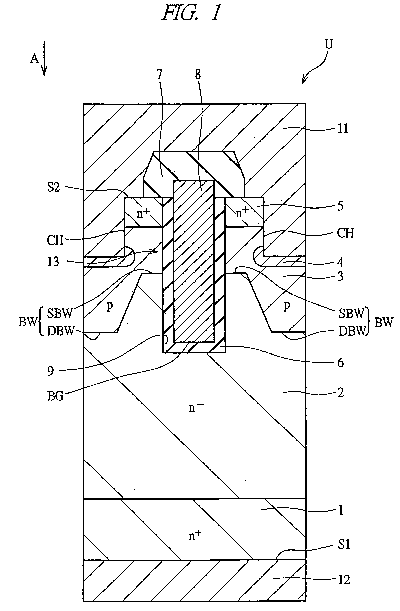
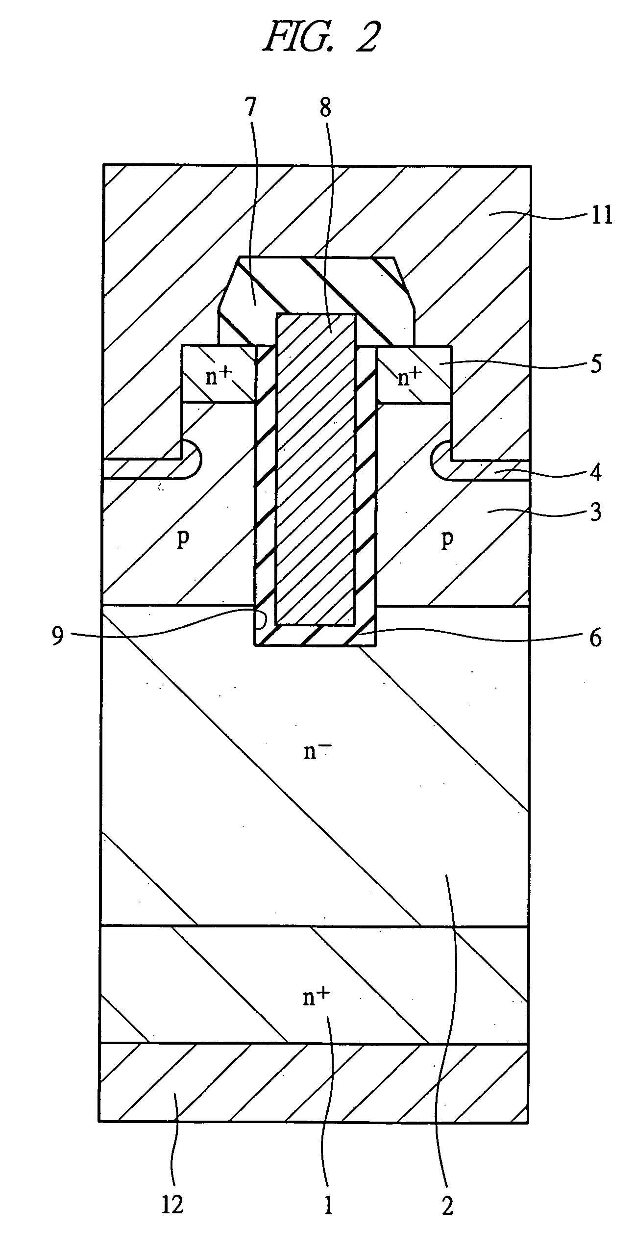
[0043]FIG. 1 is a cross-sectional view of a principal part of the trench-gate type field-effect transistor exemplified in the first embodiment. Reference numeral 1 denotes an n+-type silicon substrate (semiconductor substrate), reference numeral 2 denotes an n−-type silicon region (first semiconductor region), reference numeral 3 denotes a p-type well (semiconductor well region), reference numeral 4 denotes a p+-type semiconductor region, reference numeral 5 denotes an n+-type semiconductor region (second semiconductor region), reference numeral 6 denotes a gate oxide film (gate insulating film), reference numeral 7 denotes an insulating film, reference numeral 8 denotes a gate electrode, reference numeral 9 denotes a trench (trench portion), reference numeral 11 denotes a source electrode, and reference numeral 12 denotes a drain electrode.

[0044]Here, n-type (fi...

second embodiment

[0107]In a second embodiment, there will be described an example in which the field-effect power transistor having a low channel resistance exemplified in the first embodiment is applied to a power supply apparatus.

[0108]FIG. 14 shows a power supply circuit in the power supply apparatus of synchronous rectification system for supplying a power to a semiconductor device. In the second embodiment, for example, a processor is used as a semiconductor device to be supplied with a power. Vin denotes a DC voltage source, GND denotes a ground potential, Cin denotes an input capacity, QH1 denotes a high-side field-effect transistor (first field-effect transistor), QL1 denotes a low-side field-effect transistor (second field-effect transistor), DP1 denotes a diode incorporated in the high-side field-effect transistor QH1, DP2 denotes a diode incorporated in the low-side field-effect transistor QL1, L denotes an output inductor, Cut denotes an output capacity, 31 denotes a power supply control...


PUM


Abstract

A semiconductor device comprises a trench-gate type field-effect transistor on a semiconductor substrate having a first main surface and a second main surface oppositely positioned in a thickness direction, wherein the trench-gate type field-effect transistor comprises a first semiconductor region at the first main surface side; a second semiconductor region at the second main surface; a semiconductor well region between the first semiconductor region and the second semiconductor region; a trench formed so as to protrude in a first direction intersecting the second main surface; a gate electrode formed on an inner surface of the trench via a gate insulating film, and a bottom of the gate electrode is in the first semiconductor region, and a well bottom has a well deep portion and a well shallow portion, and the well deep portion is in a region more distant from the gate insulating film compared to the well shallow portion.

Description

CROSS-REFERENCE TO RELATED APPLICATION[0001]The present application claims priority from Japanese Patent Application No. JP 2007-054156 filed on Mar. 5, 2007, the content of which is hereby incorporated by reference into this application.TECHNICAL FIELD OF THE INVENTION[0002]The present invention relates to a semiconductor device and manufacturing method thereof and a power supply apparatus using the same, and particularly to a technique effectively applied to a semiconductor device comprising a trench-gate type field-effect transistor.BACKGROUND OF THE INVENTION[0003]A power device, such as a so-called power transistor, like a field-effect transistor (FET) having high-voltage operation capable of coping with a large current, is widely applied to various applications for power control of industrial equipment and for power supply control of various electrical appliances.[0004]As a high-voltage technique for a power transistor having a trench-gate structure, for example, Japanese Pate...

Claims


Application Information

Patent Timeline
IPC IPC(8): H01L27/088H01L29/78H01L21/336
CPCH01L21/823437H01L21/823487H01L27/088H01L29/1095H01L29/7813H01L29/41766H01L29/4236H01L29/66727H01L29/66734H01L29/41741
Inventor HASHIMOTO, TAKAYUKIHIRAO, TAKASHISHIRAISHI, MASAKI
Owner RENESAS ELECTRONICS CORP
Why Eureka
Try Eureka