Thin film transistor, preparation method for same and array substrate

A thin-film transistor and array substrate technology, applied in the display field, can solve the problem that the TFT on-state current cannot be too large

Inactive Publication Date: 2013-09-18
BEIJING BOE OPTOELECTRONCIS TECH CO LTD
View PDF4 Cites 28 Cited by
  • Summary
  • Abstract
  • Description
  • Claims
  • Application Information

AI Technical Summary

Problems solved by technology

[0005] However, in the preparation process of the TFT array substrate, due to the limitation of the existing proce...

Method used


Image

  • Thin film transistor, preparation method for same and array substrate
  • Thin film transistor, preparation method for same and array substrate
  • Thin film transistor, preparation method for same and array substrate

Examples


Embodiment 1

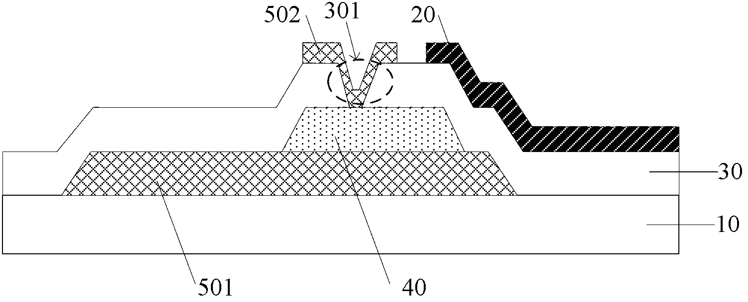
[0055] Embodiment 1 provides a thin film transistor, such as Figure 4 As shown, the thin film transistor includes: a source 501 disposed on the base substrate 10, an active layer 40 disposed above the source, a drain 502 disposed above the active layer, and a drain 502 disposed above the source There is a gate insulating layer 30 between the active layer and the drain, and a gate 20 disposed above the gate insulating layer.

[0056] Wherein, the active layer 40 includes an amorphous silicon semiconductor layer 401 in the middle, a first ohmic contact layer 402 above the amorphous silicon semiconductor layer, and a second ohmic contact layer below the amorphous silicon semiconductor layer. Layer 403.

[0057] The source 501 is in contact with the second ohmic contact layer 403 of the active layer 40, the drain 502 is in the same layer as the gate 20 but not connected, and the drain 502 is arranged on the gate The first via hole 301 on the insulating layer 30 is in contact wi...

Embodiment 2

[0060] Embodiment 2 provides a thin film transistor, such as Figure 5 As shown, the thin film transistor includes: a drain 502 disposed on the base substrate 10, an active layer 40 disposed above the drain, a source 501 disposed above the active layer, and a drain 502 disposed above the drain. There is a gate insulating layer 30 between the active layer and the source, and a gate 20 disposed above the gate insulating layer.

[0061] Wherein, the active layer 40 includes an amorphous silicon semiconductor layer 401 in the middle, a first ohmic contact layer 402 above the amorphous silicon semiconductor layer, and a second ohmic contact layer below the amorphous silicon semiconductor layer. Layer 403.

[0062] The drain 502 is in contact with the second ohmic contact layer 403 of the active layer 40, the source 501 is in the same layer as the gate 20 but not connected, and the source 501 is arranged on the gate The first via hole 301 on the insulating layer 30 is in contact w...

Embodiment 3

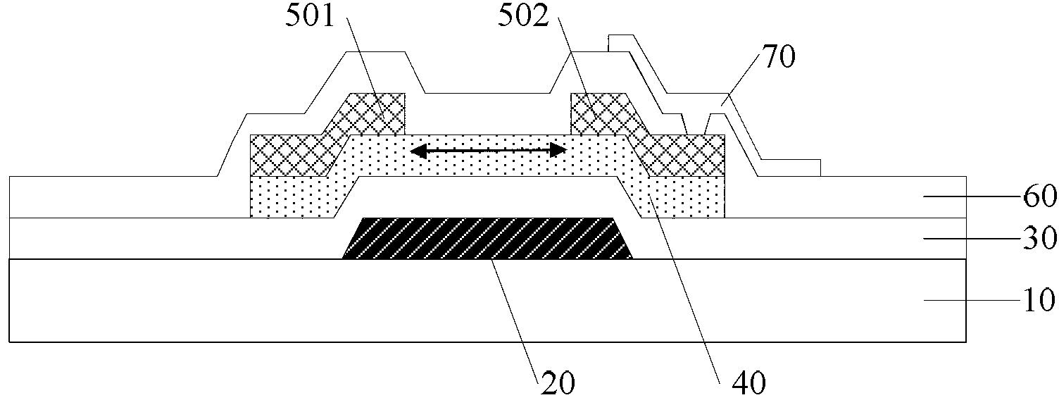
[0071] Embodiment 3 provides an array substrate, referring to Image 6 As shown, the array substrate includes from bottom to top: a base substrate 10, a source 501 disposed on the base substrate and a data line (not marked in the figure) connected to the source, and a source 501 disposed on the source The upper active layer 40, the gate insulating layer 30 arranged above the active layer 40, and the drain 502 and the gate 20 arranged on the same layer but not connected above the gate insulating layer 30, and the gate 20 A connected gate line (not marked in the figure), wherein the gate insulating layer 30 is provided with a first via hole 301, and the drain electrode 502 is in contact with the active layer 40 through the first via hole 301. In addition, it also includes: The protection layer 60 , and the pixel electrode 70 disposed on the protection layer, and the pixel electrode 70 is connected to the drain electrode 502 through the second via hole 601 disposed on the protect...


PUM


Abstract

The invention provides a thin film transistor, a preparation method for the same and an array substrate, and relates to the technical field of display. The trench length of the thin film transistor can be reduced. The thin film transistor comprises a gate arranged on a substrate, a gate insulating layer, an active layer, a source and a drain, wherein the source and the drain are arranged on the two sides of the active layer along a direction perpendicular to the substrate respectively, and contact with the active layer. The thin film transistor, the preparation method for the same and the array substrate are used for manufacturing a display.

Description

technical field [0001] The invention relates to the field of display technology, in particular to a thin film transistor, a preparation method thereof, and an array substrate. Background technique [0002] TFT-LCD (Thin Film Transistor-Liquid Crystal Display, Thin Film Field Effect Transistor Liquid Crystal Display) has the characteristics of small size, low power consumption, and no radiation, and occupies a dominant position in the current display market. [0003] TFT array substrate is one of the important parts of liquid crystal display, its cross-sectional structure is as follows figure 1 As shown, it mainly includes a substrate 10, a gate electrode 20 disposed on the substrate 10, a gate insulating layer 30, an active layer 40, a source-drain metal layer including a source electrode 501 and a drain electrode 502, and a protective layer 60 and a pixel electrode layer. 70. [0004] The on-state current of the TFT is I on ...

Claims


Application Information

Patent Timeline
IPC IPC(8): H01L29/786H01L29/423H01L21/336H01L27/12
CPCH01L29/41733H01L29/78642H01L29/78618H01L29/78663H01L27/1259H01L29/66742H01L29/7869H01L27/1222H01L27/1225H01L27/127H01L29/78669H01L29/78696
Inventor 张文余田宗民李婧
Owner BEIJING BOE OPTOELECTRONCIS TECH CO LTD
Why Eureka
Try Eureka