Embedding layer heterojunction tunneling field effect transistor and manufacturing method thereof

A technology of tunneling field effect and embedded layer, which is applied in semiconductor/solid-state device manufacturing, semiconductor devices, electrical components, etc. The effect of large on-state current and simple preparation process

Active Publication Date: 2015-01-07
PEKING UNIV
View PDF5 Cites 9 Cited by
  • Summary
  • Abstract
  • Description
  • Claims
  • Application Information

AI Technical Summary

Problems solved by technology

However, since the staggered-layer heterojunction always has a band-band tunneling window in the off-state of the device, it will lead to a large off-state current, which will reduce the current switching ratio of the device.

Method used


Image

  • Embedding layer heterojunction tunneling field effect transistor and manufacturing method thereof
  • Embedding layer heterojunction tunneling field effect transistor and manufacturing method thereof
  • Embedding layer heterojunction tunneling field effect transistor and manufacturing method thereof

Examples


Embodiment Construction

[0049] The present invention will be further described through specific embodiments below in conjunction with the accompanying drawings.

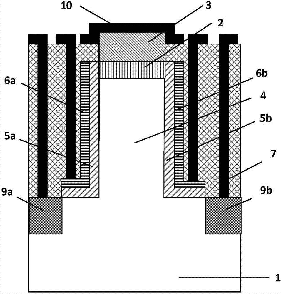
[0050] In this embodiment, the structure of the embedded layer heterojunction tunneling field effect transistor is as follows figure 1 As shown, it includes a semiconductor substrate 1 , a tunneling source region 3 , an embedded layer 2 , a channel region 4 , a drain region 9 , and a gate dielectric layer 5 and a control gate 6 located on both sides of the channel region. It is characterized in that the device has a vertical channel, and the double control gates on both sides of the vertical channel are L-shaped structures. Moreover, there is a hetero-inlaid layer 2 between the tunneling source region and the channel region. Among them, a staggered heterojunction (Broken-Gap) is formed at the interface between the tunneling source region and the embedded layer, and a staggered heterojunction (Staggered-Gap) is formed at the interface betwe...


PUM


Abstract

The invention discloses an embedding layer heterojunction tunneling field effect transistor and a manufacturing method of the embedding layer heterojunction tunneling field effect transistor, and belongs to the field of field effect transistor logic devices in the CMOS ultra large scale integration (ULSI). The two sides of a vertical channel region of the embedding layer heterojunction tunneling field effect transistor are provided with control gates respectively. The control gates are of an L-shaped structure. Gate medium layers are arranged between the two control gates and the vertical channel region. A tunneling source region is arranged above the vertical channel region. An embedding layer is arranged between the tunneling source region and the channel region. The thickness of the embedding layer is smaller than the width of a space charge region at a tunneling junction. A split-level heterojunction is formed on the interface position of the tunneling source region and the embedding layer. A staggered heterojunction is formed on the interface position of the embedding layer and the channel region. Compared with an existing TFET, by means of the embedding layer heterojunction tunneling field effect transistor, the device on-state current is increased remarkably, and the lower off-state current is kept.

Description

technical field [0001] The invention belongs to the field of CMOS ultra large scale integrated circuit (ULSI) field effect transistor logic devices, and in particular relates to an embedded layer heterojunction tunneling field effect transistor and a preparation method thereof. Background technique [0002] Since the birth of integrated circuits, microelectronics integration technology has been developing continuously in accordance with "Moore's Law", and the size of semiconductor devices has been continuously reduced. As semiconductor devices enter the deep submicron range, existing MOSFET devices are limited by the conduction mechanism of self-diffusion drift, and the subthreshold slope is limited by the thermoelectric potential kT / q, which cannot be reduced synchronously with the reduction of device size. As a result, the reduction of leakage current of MOSFET devices cannot meet the requirements of device size reduction, the energy consumption of the entire chip continue...

Claims


Application Information

Patent Timeline
IPC IPC(8): H01L29/78H01L29/06H01L21/336
CPCH01L29/0603H01L29/66484H01L29/66969H01L29/7831
Inventor 黄如吴春蕾黄芊芊王佳鑫朱昊王阳元
Owner PEKING UNIV
Why Eureka
Try Eureka