Thin film transistor and manufacturing method thereof and display device

A technology of thin film transistors and manufacturing methods, applied in the direction of transistors, semiconductor/solid-state device manufacturing, semiconductor devices, etc., can solve the problems of thin film transistors without increasing the volume of thin film transistors, and achieve the effect of increasing the on-state current

Active Publication Date: 2017-07-07
BOE TECH GRP CO LTD
View PDF4 Cites 8 Cited by
  • Summary
  • Abstract
  • Description
  • Claims
  • Application Information

AI Technical Summary

Problems solved by technology

[0005] In order to solve the problem of how to increase the on-state current of the thin film transistor without increasing the volume of the thin film transistor, an embodiment of the present invention provides a thin film transistor, a manufacturing method thereof, and a display device

Method used


Image

  • Thin film transistor and manufacturing method thereof and display device
  • Thin film transistor and manufacturing method thereof and display device
  • Thin film transistor and manufacturing method thereof and display device

Examples


Embodiment Construction

[0052] In order to make the object, technical solution and advantages of the present invention clearer, the implementation manner of the present invention will be further described in detail below in conjunction with the accompanying drawings.

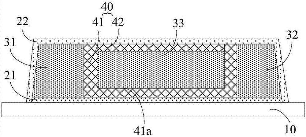
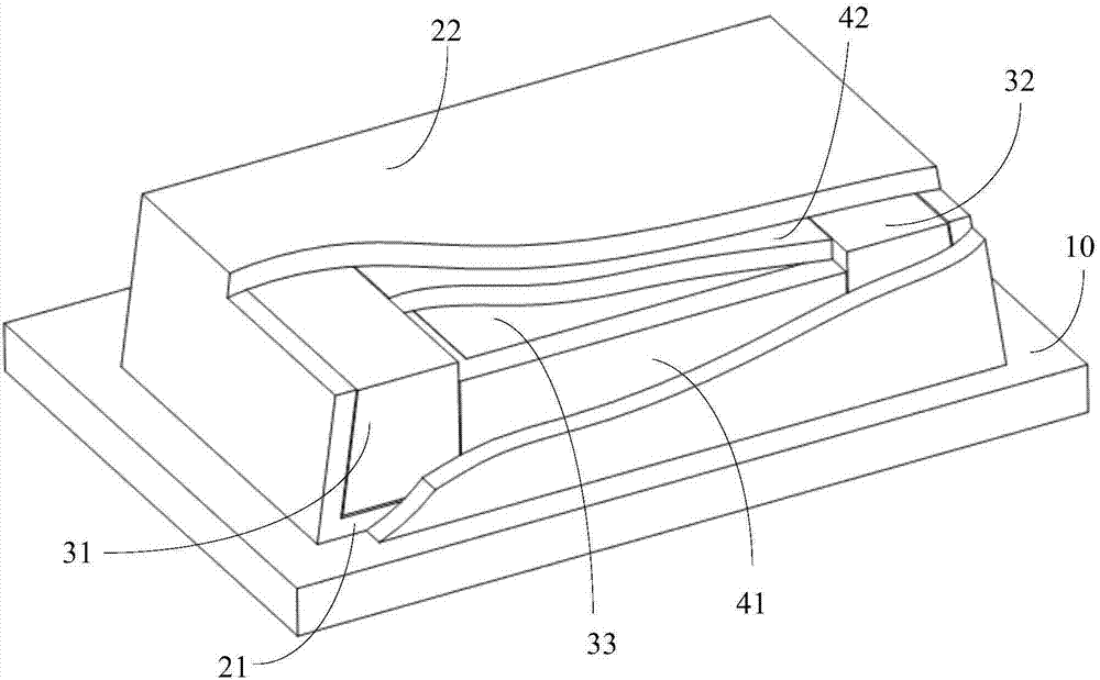
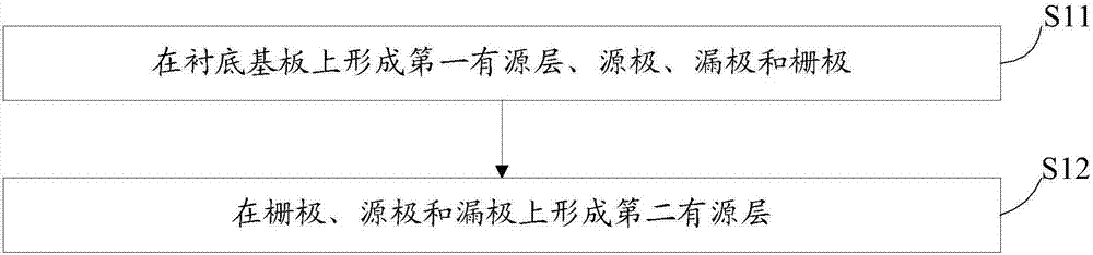
[0053] figure 1 It is a schematic structural diagram of a thin film transistor provided by an embodiment of the present invention. figure 2 is a schematic diagram of a three-dimensional structure of a thin film transistor provided by an embodiment of the present invention. For the convenience of description, figure 2 Some structures have been removed from . combine figure 1 and figure 2, the thin film transistor comprises a first active layer 21, a source 31, a drain 32, a gate 33 and a second active layer 22, wherein the source 31, the drain 32 and the gate 33 are spaced apart on the first active layer On the source layer 21, the gate 33 is located between the source 31 and the drain 32, the second active layer 22 is arranged o...


PUM


Abstract

The invention discloses a thin film transistor and a manufacturing method thereof and a display device, and belongs to the field of a semiconductor. The thin film transistor comprises a first active layer, a source electrode, a drain electrode, a grid electrode and a second active layer, wherein the source electrode, the drain electrode and the grid electrode are arranged on the first active layer at intervals; the grid electrode is arranged between the source electrode and the drain electrode; the second active layer is arranged on the grid electrode, the source electrode and the drain electrode; the source electrode and the drain electrode are connected with the first active layer and the second active layer; the grid electrode is insulated from the first active layer, the second active layer, the source electrode and the drain electrode; when a voltage is applied to the grid electrode, the source electrode and the drain electrode can be conducted through the first active layer, and the source electrode and the drain electrode can also be conducted through the second active layer; and when the source electrode and the drain electrode are conducted in the thin film transistor, the source electrode and the drain electrode can be conducted through the first active layer and the second active layer simultaneously, so that higher current can flow between the source electrode and the drain electrode, and on-state current of the thin film transistor can be improved.

Description

technical field [0001] The invention relates to the field of semiconductors, in particular to a thin film transistor, a manufacturing method thereof, and a display device. Background technique [0002] Currently common display devices include passive light-emitting display devices (such as liquid crystal display devices) and active light-emitting display devices (such as OLED (Organic Light Emitting Diode, organic light-emitting diode) display devices). Compared with the passive light-emitting display device, the active light-emitting display device has the advantages of small thickness, low power consumption, and fast response speed, so the active light-emitting display device has greater market competitiveness. [0003] The OLED display device includes a plurality of OLEDs, and each OLED is connected to a thin film transistor. The on and off of the OLED can be controlled by controlling the on and off of the thin film transistor. By adjusting the on-state current of the thi...

Claims


Application Information

Patent Timeline
Patent Type & Authority Applications(China)
IPC IPC(8): H01L29/786H01L21/336H01L29/10
CPCH01L29/1033H01L29/66742H01L29/786H01L29/66969H01L29/78696H01L29/7869H01L29/401H01L29/6675H01L29/78663H01L29/78672H01L29/78693
Inventor 王国英宋振
Owner BOE TECH GRP CO LTD
Why Eureka
Try Eureka