

Thin film transistor, manufacture method thereof, array substrate and display device
A technology of thin film transistor and substrate substrate, which is applied in the fields of thin film transistor and its manufacturing method, array substrate and display device, can solve the problems of small on-state current and low charging rate of TFT, so as to increase on-state current and improve charging rate effect
- Summary
- Abstract
- Description
- Claims
- Application Information
AI Technical Summary
Problems solved by technology
Method used
Image

Examples
Embodiment Construction
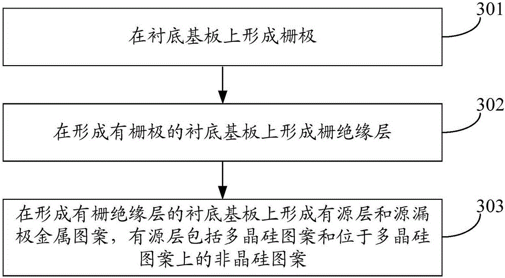
[0083] In order to make the object, technical solution and advantages of the present invention clearer, the present invention will be further described in detail below in conjunction with the accompanying drawings. Obviously, the described embodiments are only some embodiments of the present invention, rather than all embodiments . Based on the embodiments of the present invention, all other embodiments obtained by persons of ordinary skill in the art without making creative efforts belong to the protection scope of the present invention.
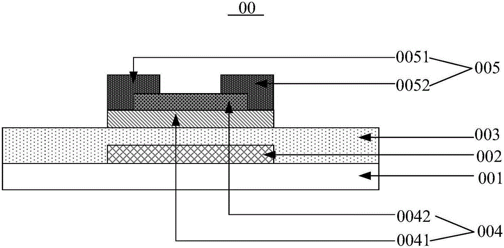
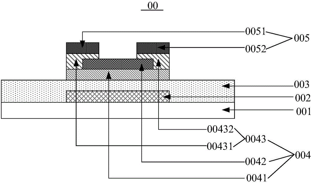
[0084] Please refer to figure 1 , which shows a schematic structural diagram of a thin film transistor 00 provided by an embodiment of the present invention, see figure 1 , the thin film transistor 00 includes: a base substrate 001 . The base substrate 001 may be a transparent substrate, specifically, a substrate made of light-guiding and non-metallic materials with a certain degree of firmness, such as glass, quartz, and transparent resi...
PUM
 Abstract
Description
Claims
Application Information