Ferro-electric field effect transistor based on structured carbon nano tube striped array and manufacturing method thereof

A carbon nanotube and electric field effect technology, applied in the field of memory, can solve the problems of cumbersome and complicated operations, small open current of ferroelectric field effect transistors, and easy mutual conduction

Inactive Publication Date: 2014-08-27
XIANGTAN UNIV
View PDF3 Cites 9 Cited by
  • Summary
  • Abstract
  • Description
  • Claims
  • Application Information

AI Technical Summary

Problems solved by technology

When a single carbon nanotube is used as the channel layer of a ferroelectric field effect transistor, the selected single carbon nanotube exhibits semiconducting properties, and is generally operated by electron beam lithography or under an atomic force microscope. Expensive and difficult to deposit source and drain electrodes; in addition, the on-state current of a ferroelectric field effect transistor with a single carbon nanotube as the channel layer is small, which brings great difficulties and complexity to the application of carbon nanotubes in devices sex

Method used


Image

  • Ferro-electric field effect transistor based on structured carbon nano tube striped array and manufacturing method thereof
  • Ferro-electric field effect transistor based on structured carbon nano tube striped array and manufacturing method thereof
  • Ferro-electric field effect transistor based on structured carbon nano tube striped array and manufacturing method thereof

Examples


Embodiment 1

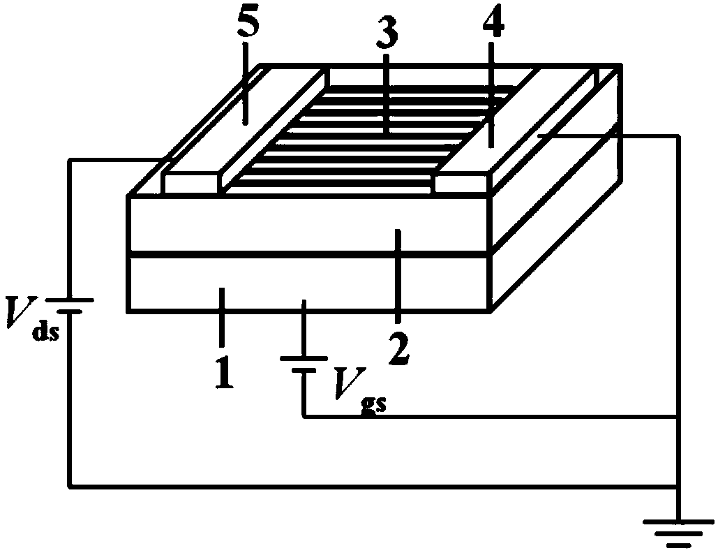
[0029] In this embodiment, Pt is used as the bottom electrode material, Bi 3.15 Nd 0.85 Ti 3 o 12 (BNT for short) is a ferroelectric field-effect transistor with a ferroelectric thin film insulating gate material, a regular MWCNT stripe array as a channel material, and Pt as a source and drain material. The specific steps are as follows:

[0030] (1) Growth of Pt bottom electrode

[0031]Clean the single crystal Si wafer, place the Pt target on the target frame, and deposit the Pt metal bottom electrode by the vacuum evaporation coating method. In order to improve the adhesion between Pt and the substrate Si, a growth Ti and SiO 2 .

[0032] (2) Growth of BNT ferroelectric thin film

[0033] Using the sol-gel method. First, prepare the BNT precursor solution. The process is: weigh 1.69785 g of bismuth nitrate crystals and 0.386495 g of neodymium nitrate powder, add them to 3 mL of glacial acetic acid until they are completely dissolved; then add 0.5 mL of acetylacetone ...

Embodiment 2

[0054] This embodiment is a ferroelectric field effect transistor with heavily doped n-type Si as the substrate and bottom electrode, BNT as the ferroelectric thin film insulating gate material, regular BWCNT stripe array as the channel material, and Pt as the source and drain materials. ,Specific steps are as follows:

[0055] (1) Growth bottom electrode

[0056] The heavily doped n-type Si is used as the substrate and bottom electrode of the ferroelectric field effect transistor.

[0057] (2) Growth of BNT ferroelectric thin film

[0058] Using the sol-gel method. The configuration process of the BNT precursor solution is the same as in Example 1, and the heat treatment process of the BNT thin film is as follows: ① 180° C., 5 minutes; ② 400° C., 5 minutes; ③ 800° C., 20 minutes. Take out the sample and continue to spin-coat the BNT film, repeat the above process 5 times, and obtain a BNT film with a uniform thickness of 340nm.

[0059] (3) Growth regular BWCNT stripe arr...

Embodiment 3

[0065] This example is to prepare a ferroelectric field effect transistor with Au as the bottom electrode material, BNT as the ferroelectric thin film insulating gate material, a regular SWCNT stripe array as the channel material, and Pt as the source and drain materials on a single crystal Si substrate. ,Specific steps are as follows:

[0066] (1) Growth of Au bottom electrode

[0067] Clean the single crystal Si wafer, place the Au target on the target frame, and deposit the Au metal bottom electrode by vacuum evaporation coating method.

[0068] (2) Growth of BNT ferroelectric thin film

[0069] Using the sol-gel method. The configuration and preparation process of the BNT precursor solution are the same as in Example 1. The heat treatment process of the BNT thin film is: ① 180°C, 5min; ② 400°C, 5min; ③ 700°C, 10min. Take out the sample and continue to spin-coat the BNT film, repeat the above process 7 times, and obtain a BNT film with a uniform thickness of 380nm.

[0...


PUM

PropertyMeasurementUnit
Widthaaaaaaaaaa
Thicknessaaaaaaaaaa
Thicknessaaaaaaaaaa

Abstract

The invention discloses a ferro-electric field effect transistor based on a structured carbon nano tube striped array and a manufacturing method of the ferro-electric field effect transistor. According to the unit structure of the transistor, a bottom electrode layer (1) is arranged on the bottom layer, a ferro-electric film insulated gate layer (2) and a structured carbon nano tube striped array channel layer (3) are sequentially arranged on the middle layer, and a top layer is arranged on the structured carbon nano tube striped array channel layer (3) and comprises a transistor source electrode (4) and a transistor drain electrode (5); carbon nano tubes are single-walled carbon nano tubes, or double-walled carbon nano tubes or multi-walled carbon nano tubes. According to the ferro-electric field effect transistor, the on-state current and the switch ratio are large, carrier mobility is high, the starting voltage is small, the storage window is wide, and meanwhile the ferro-electric field effect transistor has the advantages of being simple in structure and a buffering layer is not needed, interface contact between a ferro-electric layer and a semiconductor layer is good, and large-area soft devices are easy to obtain. The manufacturing method is simple in technology, convenient to operate and low in cost and dispense with expensive equipment, and large-area and large-scale industrial production is easy to realize.

Description

technical field [0001] The invention belongs to the technical field of memory, and in particular relates to a ferroelectric field-effect transistor based on a regular carbon nanotube stripe array and a preparation method thereof. Background technique [0002] Ferroelectric memory has the advantages of non-volatility, low power, high read and write speed, high storage density, excellent radiation resistance, etc., and has very broad application prospects in the fields of electronic information, aerospace, instrumentation, and national defense. Transistor-type ferroelectric memory is an ideal configuration of ferroelectric memory. Its unit is only composed of a ferroelectric field effect transistor (FeFET). Compared with capacitive ferroelectric memory, it has non-destructive properties. It has the advantages of permanent readout, simple structure, higher storage density, and lower power consumption. The ferroelectric field effect transistor uses a ferroelectric thin film as ...

Claims


Application Information

Patent Timeline
IPC IPC(8): H01L29/78H01L29/41H01L21/336
CPCH01L29/6684B82Y10/00H01L29/1033
Inventor 钟向丽刘盼盼宋宏甲王金斌李波周益春
Owner XIANGTAN UNIV
Why Eureka
Try Eureka