

Oxide thin film transistor, manufacturing method thereof, array substrate and display device
A technology of oxide film and manufacturing method, which is applied in the direction of transistor, semiconductor/solid-state device manufacturing, electric solid-state device, etc., and can solve the problems of long and difficult channel length
- Summary
- Abstract
- Description
- Claims
- Application Information
AI Technical Summary
Problems solved by technology
Method used
Image

Examples
Embodiment 1
[0040] In order to solve the above technical problems, an embodiment of the present invention provides a method for fabricating an oxide thin film transistor, which includes:
[0041] 110: sequentially forming a gate and a gate insulating layer on the substrate.
[0042] 120: Form an oxide semiconductor thin film on the gate insulating layer, form a first photoresist in the active layer region, and make the thickness of the first photoresist in the channel region greater than that of the first photoresist in the non-channel region glue;
[0043] 130: removing the oxide semiconductor film in the non-active layer region, forming a pattern of the active layer, removing the first photoresist in the non-channel region, and retaining the first photoresist in the channel region;
[0044] 140: Form a source-drain metal film and a second photoresist sequentially above the pattern of the active layer, and remove part of the source-drain metal film corresponding to the remaining first p...
Embodiment 2
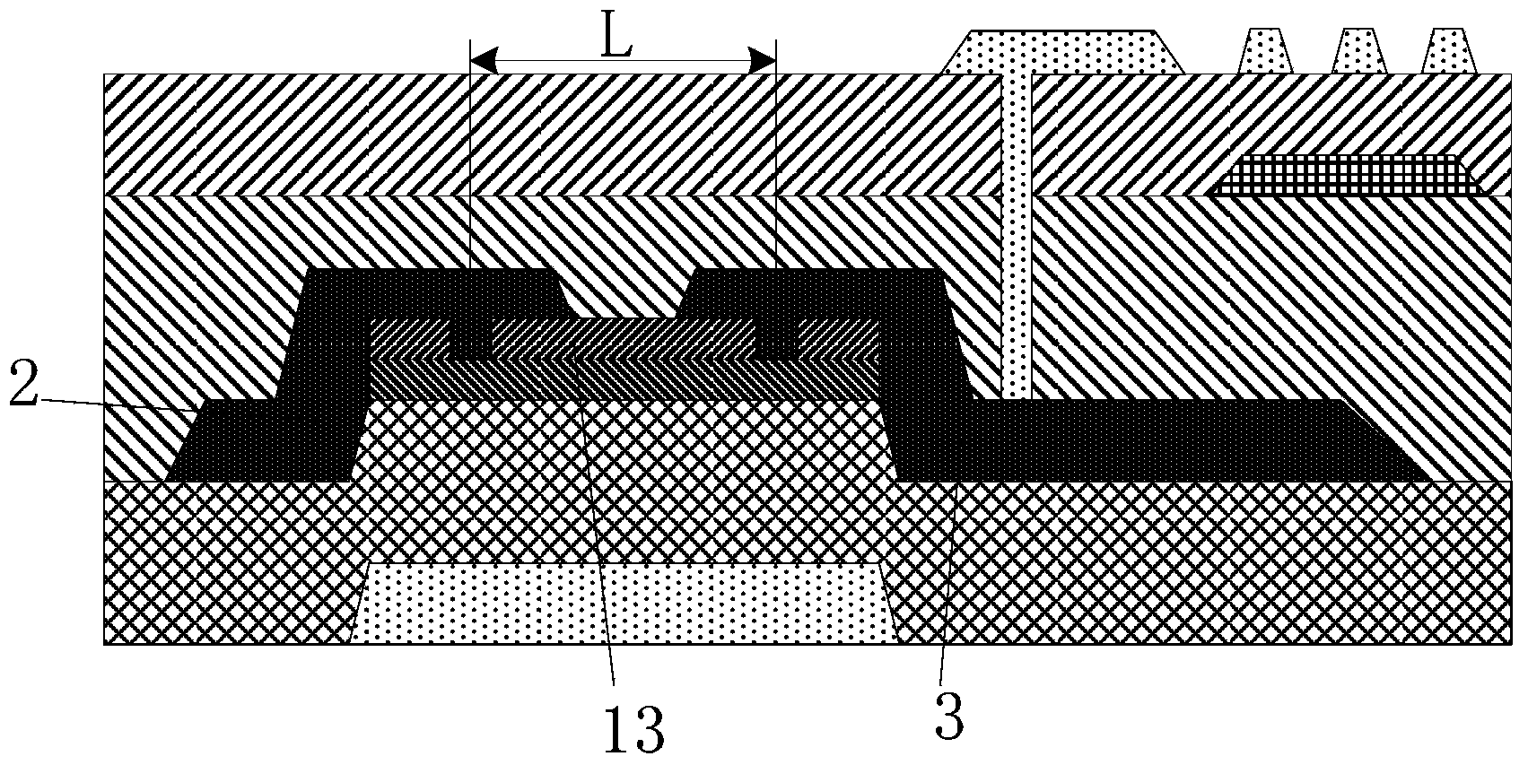
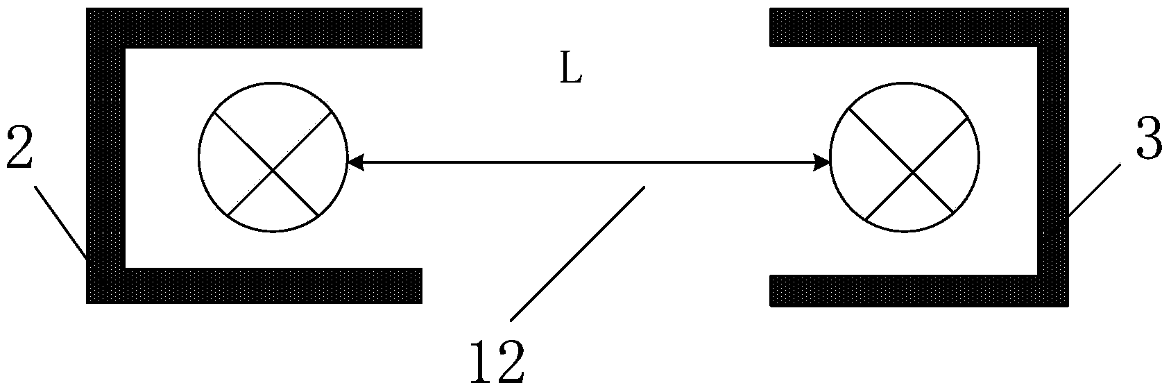
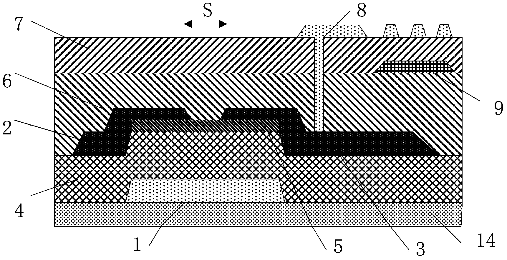
[0065] An embodiment of the present invention also provides an oxide thin film transistor, such as image 3 , Figure 4 shown, including:
[0066] A gate 1 is sequentially formed from one side of the substrate 14 , a gate insulating layer 4 is formed on a side of the gate 1 away from the substrate 14 , and an active layer 5 is formed on a side of the gate insulating layer 4 away from the gate 1 .
[0067] A source 2 and a drain 3 are formed on the side of the active layer 5 away from the gate insulating layer 4, and both the source 2 and the drain 3 are directly connected to the active layer 5. The source layer 5 is an oxide semiconductor material, such as IGZO.
[0068] The length S of the channel 12 between the source 2 and the drain 3 is 5-6um. Specifically, if the current precision allows, the distance between the source 2 and the drain 3 is 3 μm, and the width of the source 2 in the channel region is 1-1.5 μm. μm, the width of the drain 3 in the channel region is 1˜1....
Embodiment 3
[0076] An embodiment of the present invention also provides an array substrate, including the oxide thin film transistor described in Embodiment 2 above.
PUM
 Abstract
Description
Claims
Application Information