

Method of forming a metal gate in a semiconductor device
a metal gate and semiconductor technology, applied in the direction of semiconductor devices, electrical devices, transistors, etc., can solve the problems of insufficient precision control of the line width of the pattern to be formed, the inability to reduce the resolution limit of the gate electrode, and the limited use of polysilicon, so as to reduce the electrical resistance of the gate electrode and reduce the channel length of the transistor
- Summary
- Abstract
- Description
- Claims
- Application Information
AI Technical Summary
Benefits of technology
Problems solved by technology
Method used
Image

Examples
embodiment 1
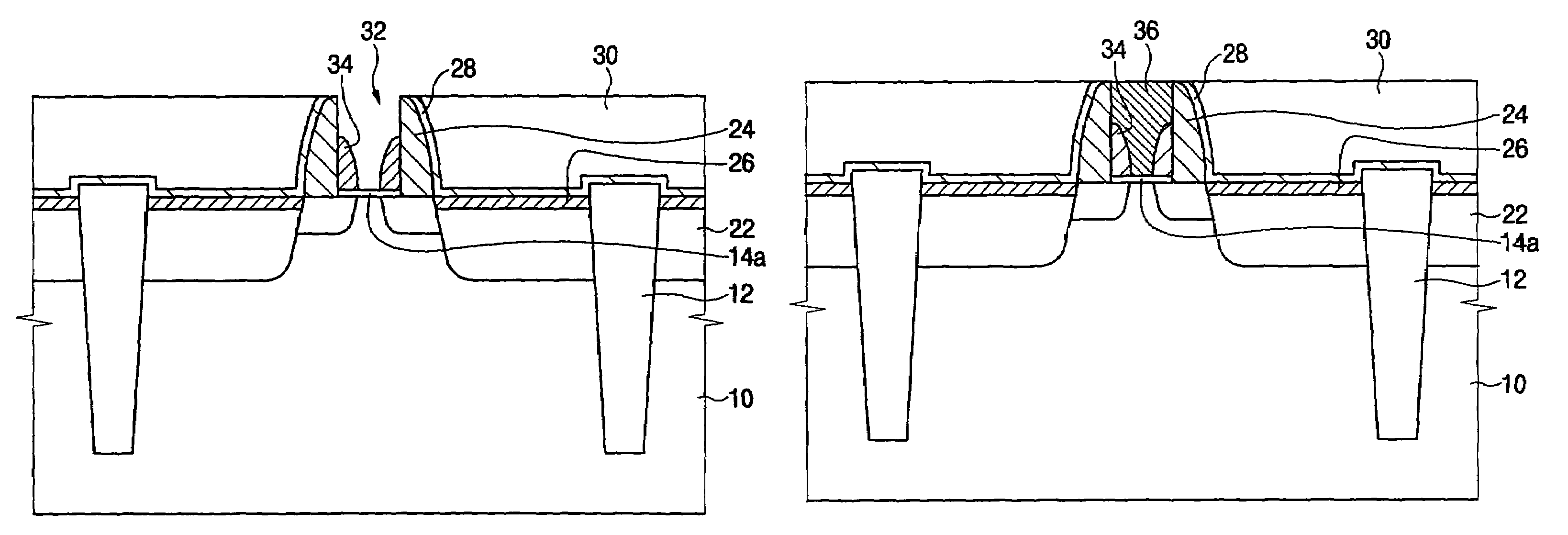
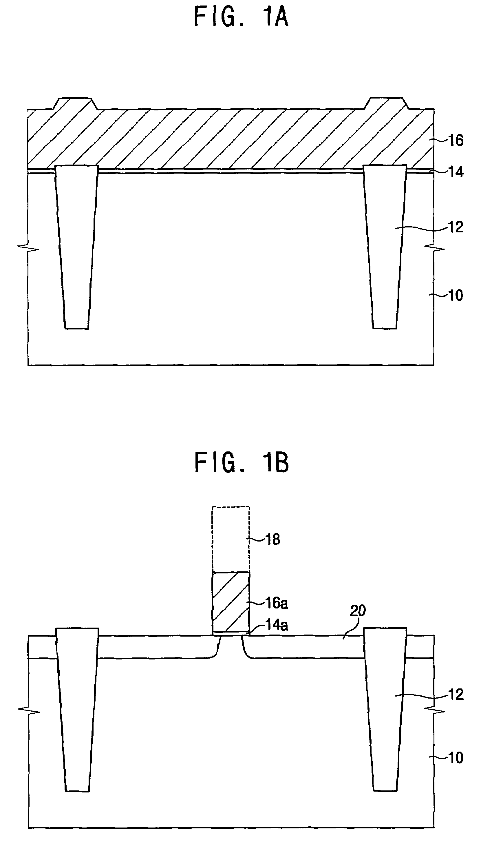
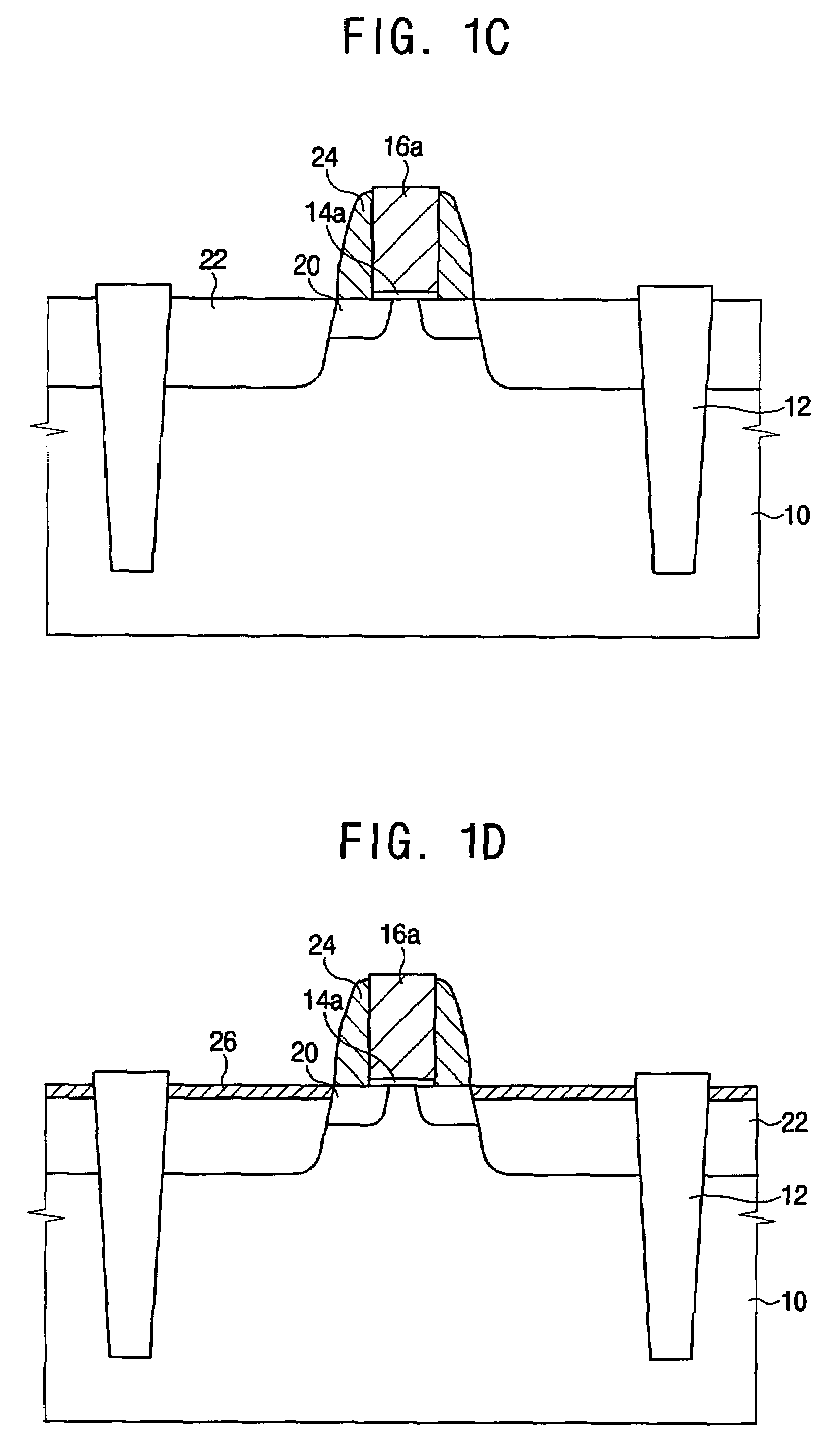
[0033]FIGS. 1A to 1I are cross sectional views showing processing steps of a method of forming a metal gate according to a first embodiment of the present invention.
[0034]Referring to FIG. 1A, a device isolation process such as a shallow trench isolation (STI) process is performed on a semiconductor substrate 10; thus an active region and a field region 12 are defined on the substrate 10. Then, an ion implantation process is performed on the substrate 10, thereby forming a well region and a channel region on the substrate 10. Agate oxide layer 14 is formed on the substrate on which the active region and field region are defined.
[0035]A dummy gate layer 16 is formed on the gate oxide layer 14 so as to form a gate pattern on the gate oxide layer 14. The dummy gate layer 16 comprises an insulation material having an etching selectivity with respect to the gate oxide layer 14. For example, the dummy gate layer 16 comprises a nitride-based material such as silicon oxynitride (SiON) or si...
embodiment 2
[0059]FIGS. 2A to 2E are cross sectional views showing processing steps of a method of forming a metal gate according to a second embodiment of the present invention. The second embodiment of the present invention as will be described hereinafter is the same as the first embodiment of the present invention except that the first spacer and the ion implantation using the first spacer as a mask are omitted. Thus, the same reference numerals in the present embodiment denote the same elements in the first embodiment of the invention, and the detailed descriptions of the same elements will be omitted to avoid a redundancy.
[0060]Referring to FIG. 2A, a device isolation process such as a shallow trench isolation (STI) process is performed on a semiconductor substrate 10, thus an active region and a field region 12 are defined on the substrate 10. Then, an ion implantation process is performed on the substrate 10, thereby forming a well region and a channel region on the substrate 10. A gate...
embodiment 3
[0071]FIGS. 3A to 3D are cross sectional views showing processing steps of a method of forming a metal gate according to a third embodiment of the present invention. The third embodiment of the present invention as will be described hereinafter is the same as the first embodiment of the present invention except that an offset spacer is formed. Thus, the same reference numerals in the present embodiment denote the same elements in the first embodiment of the invention, and the detailed descriptions of formation of the same elements will be omitted to avoid redundancy.
[0072]Referring to FIG. 3A, a device isolation process such as a shallow trench isolation (STI) process is performed on a semiconductor substrate 10, thus an active region and a field region 12 are defined on the substrate 10. Then, an ion implantation process is performed on the substrate 10, thereby forming a well region and a channel region on the substrate 10. A gate oxide layer and a dummy gate layer are formed on t...
PUM
 Abstract
Description
Claims
Application Information