Ferroelectric non-volatile memory device having integral capacitor and gate electrode, and driving method of a ferroelectric non-volatile memory device

a non-volatile memory, ferroelectric technology, applied in semiconductor devices, digital storage, instruments, etc., can solve the problems of data destruction in non-selected memory cells, inability to select memory cells, and difficult to determine the on/off state of selected memory cells cij, so as to improve the coupling ratio, reduce the length of channels, and increase the high-speed operation of transistors

Inactive Publication Date: 2005-05-24
SEIKO NPC +1
View PDF7 Cites 34 Cited by
  • Summary
  • Abstract
  • Description
  • Claims
  • Application Information

AI Technical Summary

Benefits of technology

[0040]According to the second aspect of the invention, similarly to the first aspect of the invention, the coupling ratio can be increased without increasing the area of the gate electrode of the MIS-FET. In addition, one electrode of the second capacitor is integrally formed with the floating gate so as to overlap a part of the source region excluding the boundary between the channel region and the source region, and the other electrode of the second capacitor is made of the source region. Therefore, the second capacitor is integrally formed with the MIS-FET at the connection portion with the MIS-FET, and additional interconnection is not necessary. A margin for positioning of the otherwise required interconnection is not necessary either. Therefore, unwanted increase in the area of the memory cell can be avoided. One electrode, as upper electrode, of the second capacitor does not overlap the boundary between the source region and the channel region, so that using this part and the gate electrode as a mask, the source region can be formed by self-alignment process. The boundary region between the source region and the channel region can be aligned with the end of the floating gate without any special process. More specifically, the channel length can be reduced to the minimum fabrication dimension in the LSI manufacturing process and thus good transistor characteristics can be provided.
[0051]In the ferroelectric non-volatile memory device according to the tenth to twelfth aspects of the invention, the floating gate and the ferroelectric capacitor are manufactured separately, and therefore residue of the ferroelectrics for example does not adversely affect the MIS-FET that is produced in the preceding process, so that good transistor characteristics can be provided. The first and second capacitors are formed one on the other in the vertical direction, and therefore interconnection in the horizontal direction of the semiconductor substrate is not necessary. This allows the occupied area to be reduced as much as possible, one electrode of each of the capacitors can be directly placed on one electrode of the other capacitor or may be formed integrally if necessary, so that the interconnection process is entirely done away with and the manufacturing process may be simplified as much as possible.

Problems solved by technology

When the electric field caused at the ferroelectric thin film by the voltage Vf is not more than the coercive electric field, sufficient polarization inversion is not caused, and therefore the device does not function as a memory.
(1) At the time of data writing, when the word line WLi connected to the memory cell Cij to which data is to be written is selected, writing voltage is applied from the word line WLi to all the memory cells connected to the word lines WLi, and data is written in the memory cells. The memory cell for writing cannot be selected.
(2) At the time of data erasure, the word line WLi connected to the memory cell Cij whose data is to be erased is selected, erasure voltage from the word line WLi is applied to all the memory cells connected to the word line WLi and data in the memory cells is rewritten. Therefore, the memory cell cannot be selected.
(3) At the time of data reading, when the bit line BLj and the source line SLj connected to the memory cell Cij from which data is to be read out are selected, and non-selected memory cells connected to the bit line BLj and the source line SLj are in an on state, current is passed between the bit line BLj and the source line SLj through the non-selected cells. This makes it difficult to determine the on / off state of the selected memory cell Cij.
(4) At the time of reading, when voltage is applied to the word line WLi connected to the memory cell Cij from which data is to be read out in order to select the cell, unwanted voltage is applied to non-selected memory cells similarly connected to the word line WLi, and data in the non-selected memory cells is destroyed.
(5) Negative (−) voltage is necessary in addition to positive (+) voltage in order to invert the polarization. In this case, an additional negative voltage generation circuit or negative voltage generation means provided outside the chip is necessary, which increases the chip area or the number of necessary parts.
According to this conventional method, however, the disadvantage (5) cannot be solved, and when voltage continues to be applied to non-selected memory cells in the direction to invert the polarization, the polarization is inverted, which could give rise to eventual re-writing with wrong data.
According to the latter method, it would be extremely difficult to secure a registration margin when contact holes for Al electrode interconnection to the upper electrode of the ferroelectric capacitor are formed.
The former method can however increase current leakage or lower breakdown voltage.
The latter method restricts flexibility in designing the circuit of the data detection MIS field effect transistor 101.
However, Japanese Patent No. 2,800,745, and JP-A Nos. 7-202138 and 2000-349251 do not disclose how to write, read, and erase data to / from a memory cell independently from the other memory cells.
Therefore, these disclosed methods still suffer from the disadvantages (1) to (5) in writing, reading, erasing data to / from a memory cell.

Method used


Image

  • Ferroelectric non-volatile memory device having integral capacitor and gate electrode, and driving method of a ferroelectric non-volatile memory device
  • Ferroelectric non-volatile memory device having integral capacitor and gate electrode, and driving method of a ferroelectric non-volatile memory device
  • Ferroelectric non-volatile memory device having integral capacitor and gate electrode, and driving method of a ferroelectric non-volatile memory device

Examples


Embodiment Construction

[0069]Now, the best mode to carry out the invention will be described in conjunction with the accompanying drawings.

Embodiments of the Invention

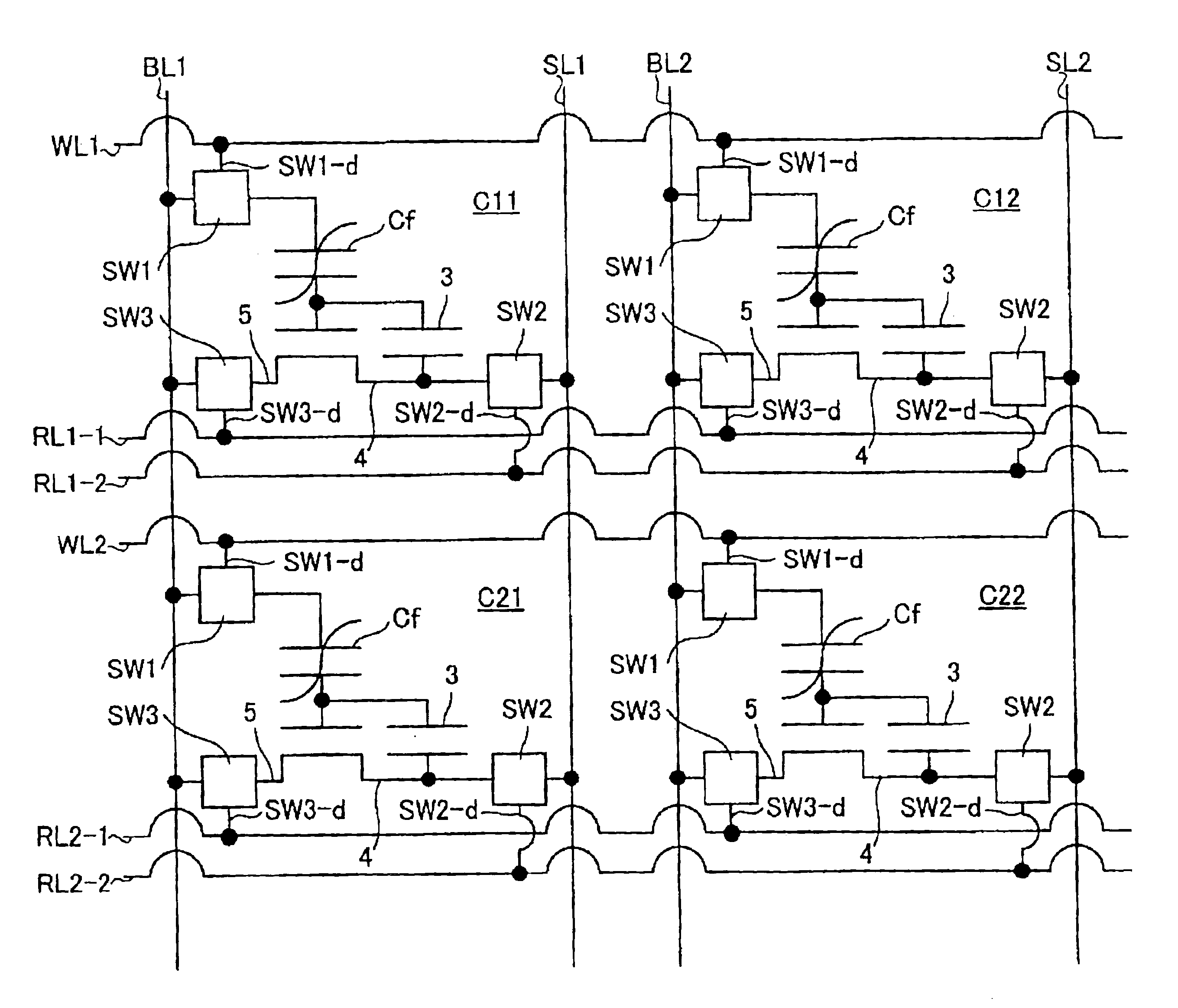
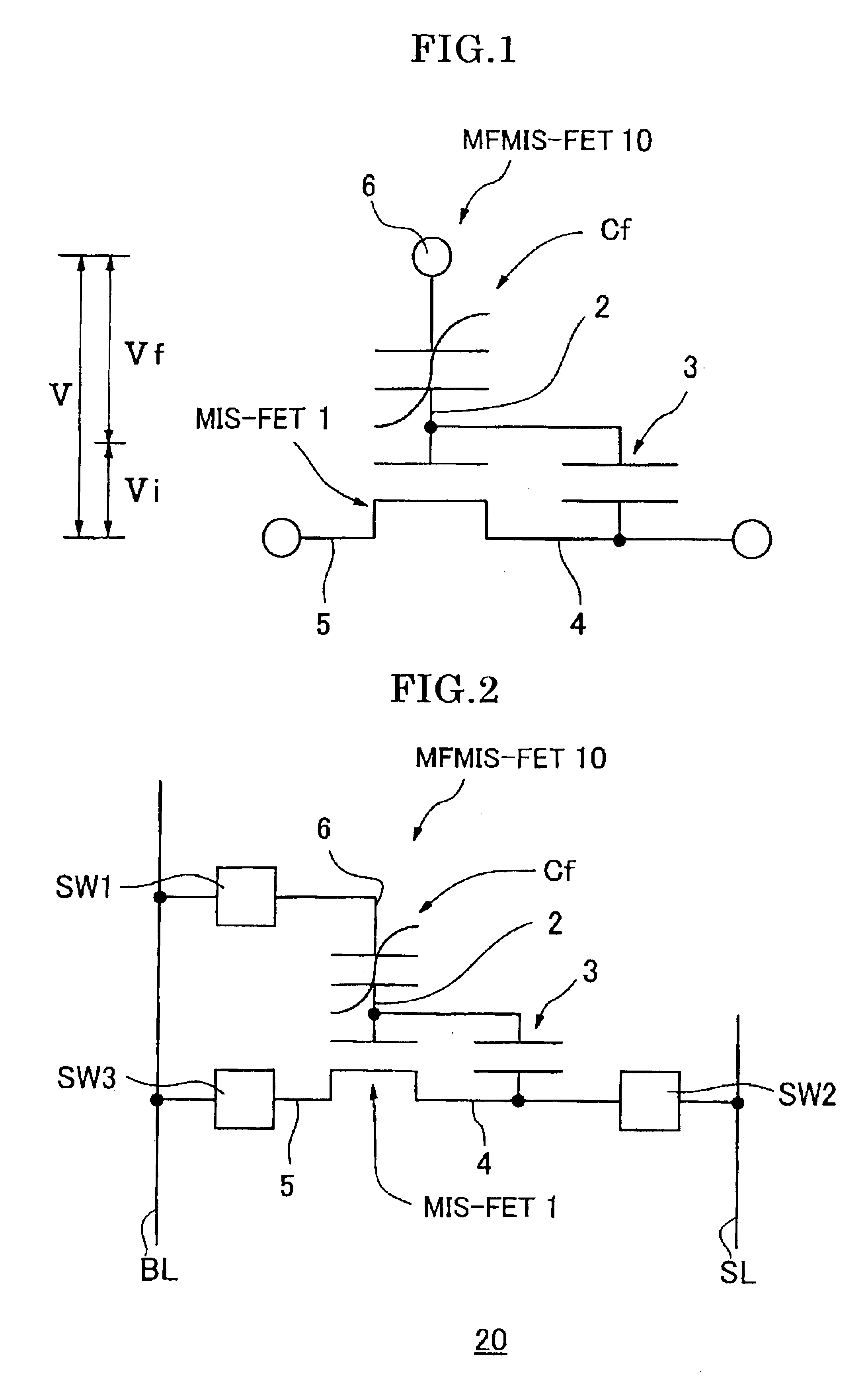
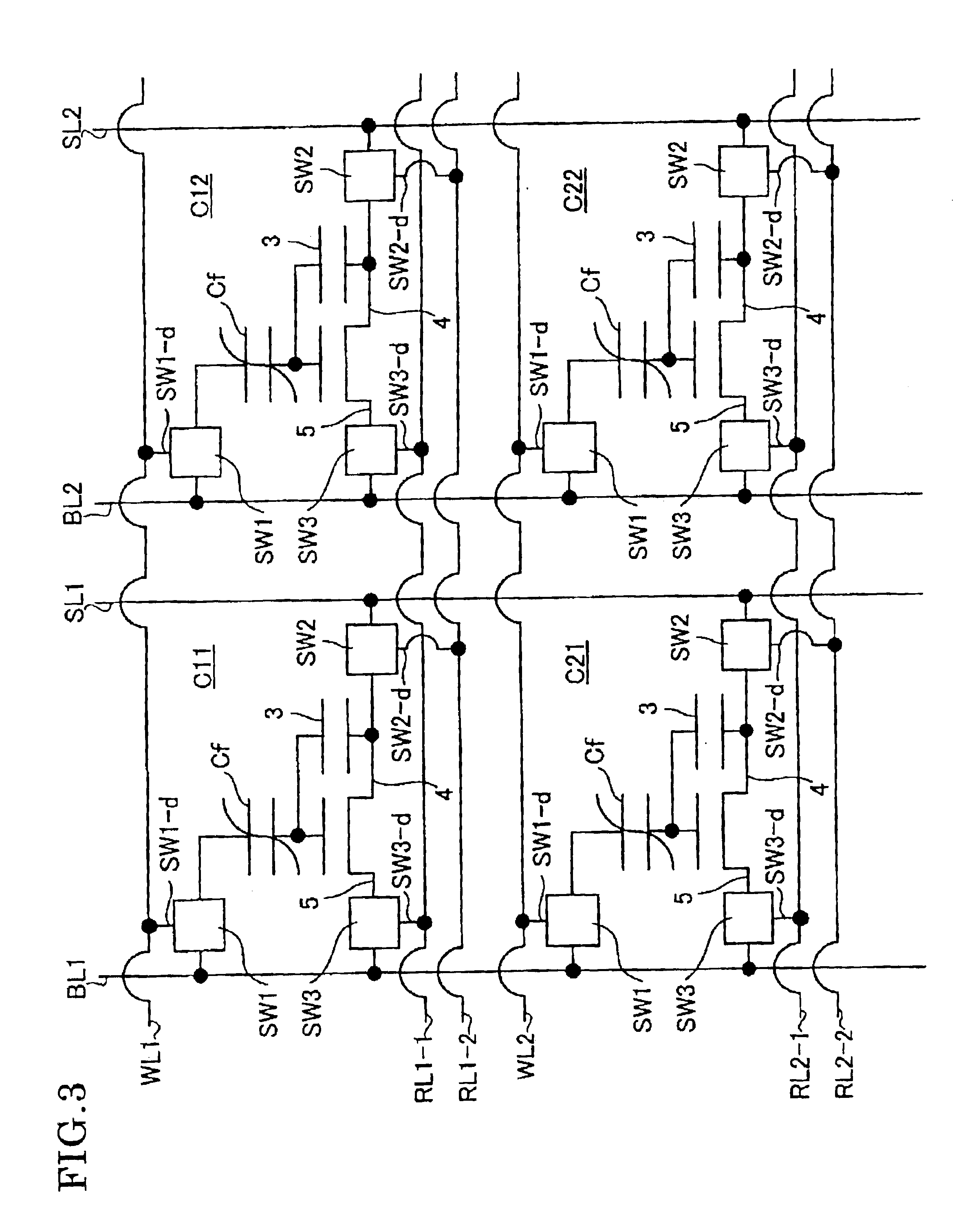
[0070]FIG. 1 is an equivalent circuit diagram of a ferroelectric, non-volatile memory transistor according to the invention. In an MFMIS (Metal Ferroelectric Metal Insulator Semiconductor)-FET (Field Effect Transistor) 10, a floating gate electrode 2 is provided between a ferroelectric capacitor Cf as a first capacitor of a thin film of ferroelectrics such as SBT (SrBi2Ta2O9) and a gate insulator. The floating gate electrode 2 is connected with one terminal of a paraelectric capacitor 3 as a second capacitor, and the terminal of the paraelectric capacitor 3 on the opposite side to the terminal connected to the floating gate electrode 2 is connected to the source 4 of the MIS (Metal Insulator Semiconductor) field effect transistor 1 (hereinafter simply as “MIS-FET”). More specifically, the memory cell includes the first and second capacitors ...


PUM


Abstract

A ferroelectric non-volatile memory device that allows the coupling ratio to be increased and the effect of voltage distribution to the ferroelectric capacitor to be improved without increasing the area of the gate electrode of a detection MIS field effect transistor is provided. In a memory cell structure, a semiconductor including regions for a source, a channel, and a drain, a gate insulator on the channel region, a floating gate conductor, a ferroelectrics, and an upper electrode conductor are layered in this order. The structure includes a paraelectric capacitor having one end connected to the floating gate conductor and the other end connected to the source region.

Description

BACKGROUND OF THE INVENTION[0001]1. Field of the Invention[0002]The present invention relates to a ferroelectric non-volatile memory device including non-destructive reading, transistor type ferroelectric memory cells arranged in a matrix of rows and columns and having a ferroelectrics for each control gate, and a driving method thereof.[0003]2. Description of the Related Art[0004]One such conventional non-destructive reading, ferroelectric non-volatile memory device is an MFMIS (Metal Ferroelectric Metal Insulator Semiconductor)-FET (Field Effect Transistor) 104 as shown in FIG. 13. In the MFMIS-FET 104, an MIS (Metal Insulator Semiconductor) field effect transistor 101 is formed on a semiconductor substrate 100, and a gate electrode (floating gate electrode) 102 on the gate insulator 109 of the transistor 101 is connected in series with a ferroelectric capacitor Cf including a ferroelectric thin film 103 made of for example PZT (PbZrTiO3) or SBT (SrBi2Ta2O9) and an upper electrode...

Claims


Application Information

Patent Timeline
Patent Type & Authority Patents(United States)
IPC IPC(8): G11C11/22H01L21/8246H01L21/8247H01L27/105H01L29/788H01L29/792
CPCG11C11/22
Inventor SAKAI, SHIGEKISAKAMAKI, KAZUO
Owner SEIKO NPC
Why Eureka
Try Eureka