

Shift register and image display apparatus containing the same
a technology of image display apparatus and shift register, which is applied in the field of shift register to achieve the effect of improving driving reliability and increasing circuit area
- Summary
- Abstract
- Description
- Claims
- Application Information
AI Technical Summary
Benefits of technology
Problems solved by technology
Method used
Image

Examples
first preferred embodiment
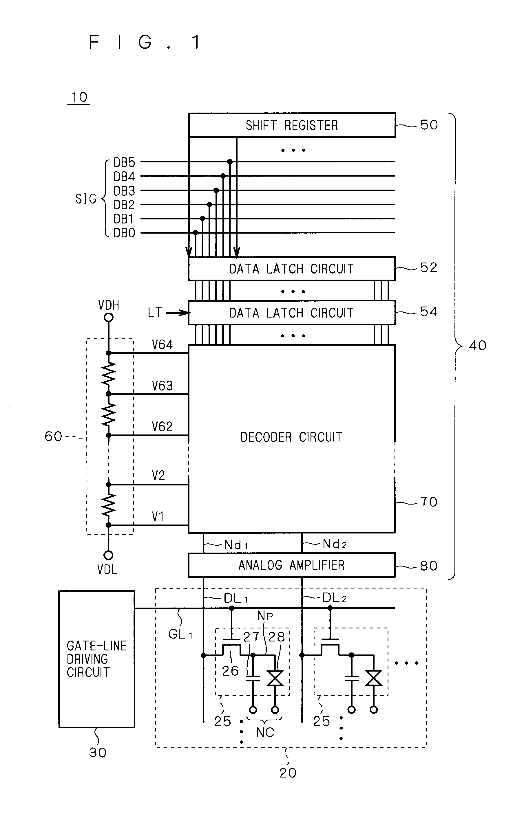
[0057]FIG. 1 is a schematic block diagram illustrating the configuration of a display apparatus according to the present invention. The overall configuration of a liquid crystal display 10 is shown as an representative example of the display apparatus.
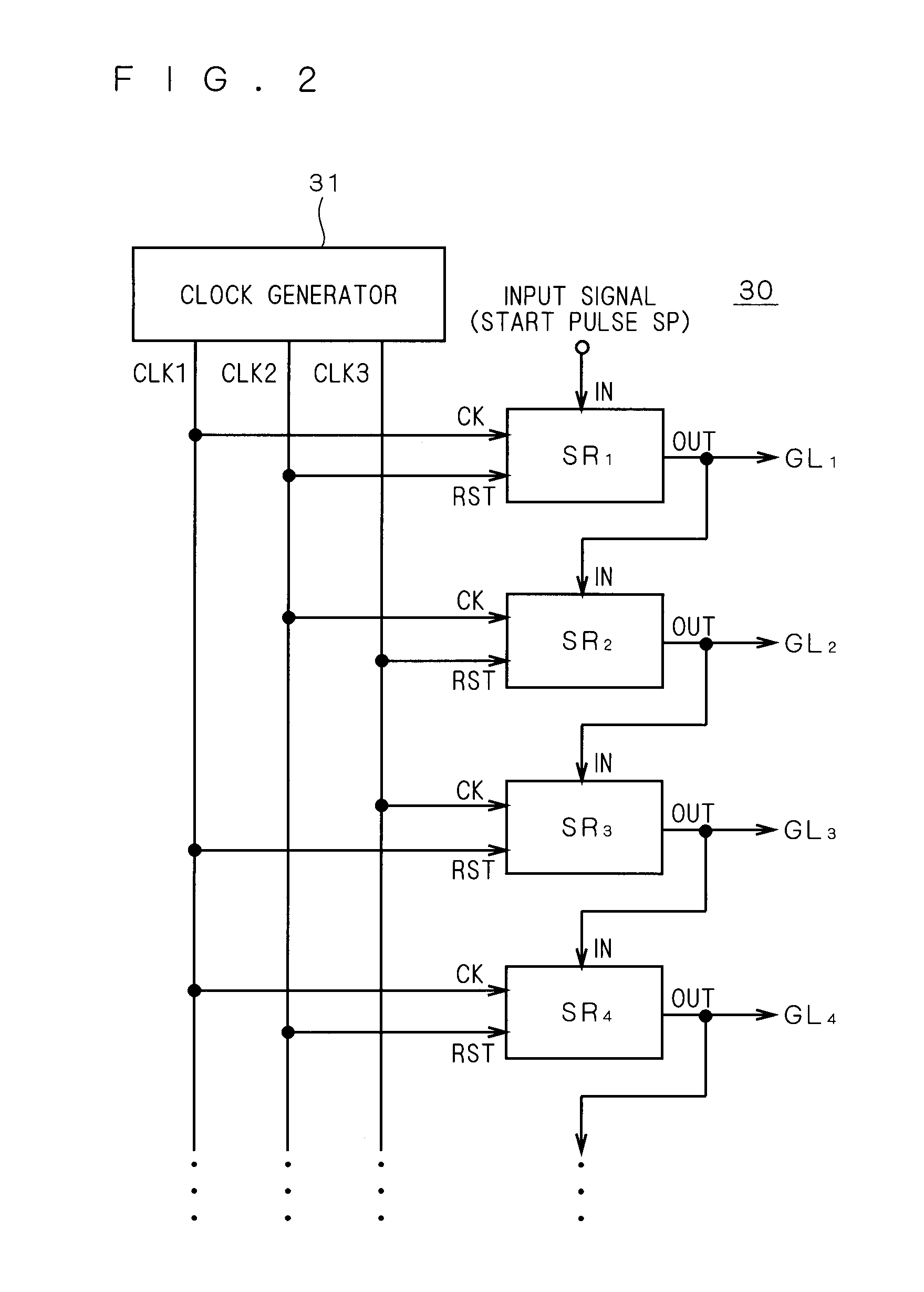
[0058]The liquid crystal display 10 is provided with a liquid crystal array part 20, a gate-line driving circuit (scanning-line driving circuit) 30 and a source driver 40. As will become apparent from the following description, a shift register according to the present invention is mounted on the gate-line driving circuit 30.
[0059]The liquid crystal array part 20 includes a plurality of pixels 25 arrayed in a matrix. The columns of pixels (hereinafter also referred to as “pixel lines”) are respectively provided with gate lines GL1, GL2, #. . . (hereinafter also generically referred to as a “gate line GL”), and the rows of pixels (hereinafter also referred to as “pixel rows”) are respectively provided with data lines DL1, DL2, #. . . (h...
third preferred embodiment
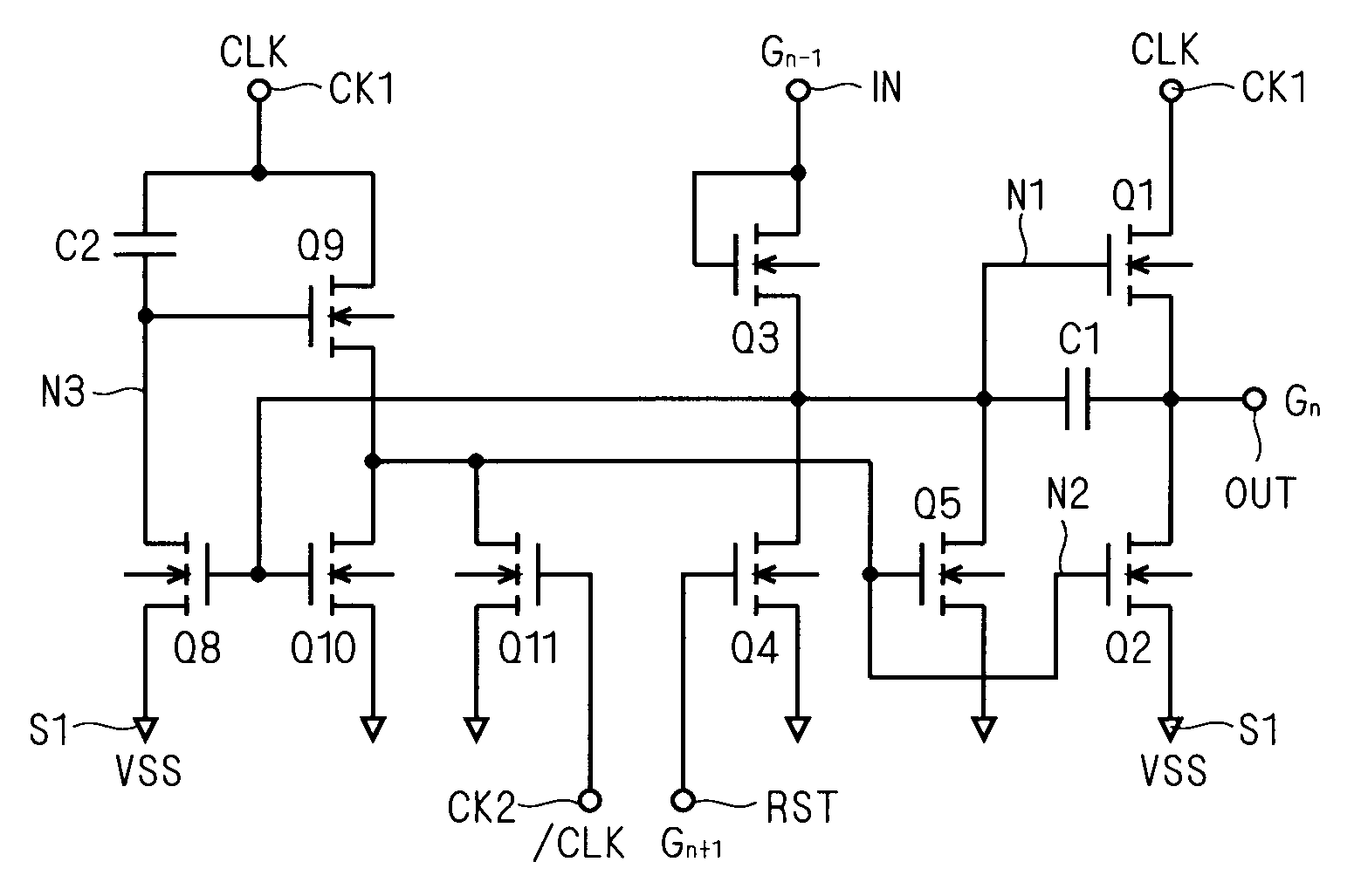
[0146]FIG. 11 is a circuit diagram illustrating the configuration of a unit shift register according to a third preferred embodiment of the present invention. In this drawing, elements having similar functions as those shown in FIG. 7 are indicated by the same reference characters. The gate node of the transistor Q8, i.e., the input node of the inverter circuit is defined as a “node N1A”. While the gate of the transistor Q1 (node N1) and node N1A are directly connected in the first preferred embodiment (FIG. 7), a transistor Q12 with its gate connected to the node N1A is diode-connected between the nodes N1 and N1A in the unit shift register SR shown in FIG. 11. Further, a transistor Q13 with its gate connected to the input terminal IN is diode-connected between the node N1A and input terminal IN.
[0147]In the unit shift register SRn according to the present embodiment, the node N1 is charged to the H level (VDD−Vth) through the transistor Q3 when the output signal Gn−1 from the imme...
sixth preferred embodiment
[0159]As described, according to the fifth preferred embodiment, the period in which the output terminal OUT is at the L level with high impedance in the non-selected period can be reduced. However, in the case where there is a certain interval between the period in which the clock signal CLK is at the H level (active period) and the period in which the clock signal / CLK is at the H level as in the example shown in FIG. 9, there is a certain period in which the output terminal OUT is at the L level with high impedance in the non-selected period. For instance, in the unit shift register SRn shown in FIG. 14, there is a period in which the node N2 and clock signal / CLK are both at the L level as shown in FIG. 17A between the rising of the clock signal CLK and the rising of the clock signal / CLK, and the transistors Q2 and Q15 are both off in that period. The output terminal OUT is thus brought into the high impedance state.
[0160]FIG. 15 is a circuit diagram illustrating the configurat...
PUM
 Abstract
Description
Claims
Application Information