Semiconductor device

A semiconductor and device technology, applied in the field of semiconductor devices including processors

Active Publication Date: 2018-05-22
RENESAS ELECTRONICS CORP
View PDF9 Cites 0 Cited by
  • Summary
  • Abstract
  • Description
  • Claims
  • Application Information

AI Technical Summary

Problems solved by technology

Peaks in power consumption and the like may be dispersed due to a delay (distribution) between timings of a plurality of processes executed by the first and second processors 10 and 20

Method used


Image

  • Semiconductor device
  • Semiconductor device
  • Semiconductor device

Examples


no. 1 example

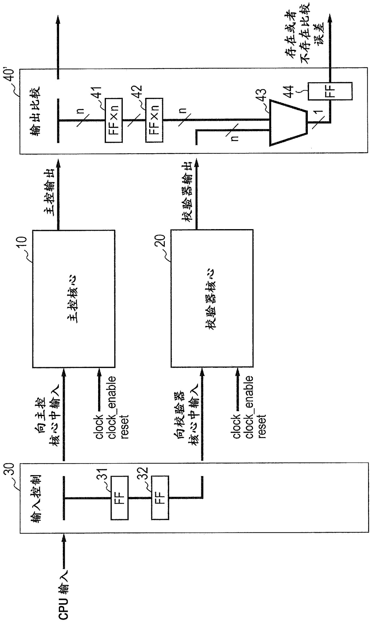
[0046] figure 2 is a diagram showing the configuration of the first embodiment of the present invention. Here, respectively to figure 2 in and figure 1 The units in the same or equivalent units are given to the figure 1 Units in are given the same reference numbers. The following will omit accordingly if necessary figure 2 The difference between figure 1 The description of the section that is repeated in the section. refer to figure 2 , this semiconductor device includes a first processor 10 and a second processor 20, an input control circuit 30 and an output comparison circuit 40 working respectively as a master control core and a checker core of a dual-core lockstep scheme. The input control circuit 30 uses two-stage flip-flops (31, 32) to delay the signal (CPU input) input to the first processor 10 by a predefined clock cycle (for example, two clock cycles) and input it to the second processor 20. delayed signal.

[0047] In the output comparison circuit 40,...

no. 2 example

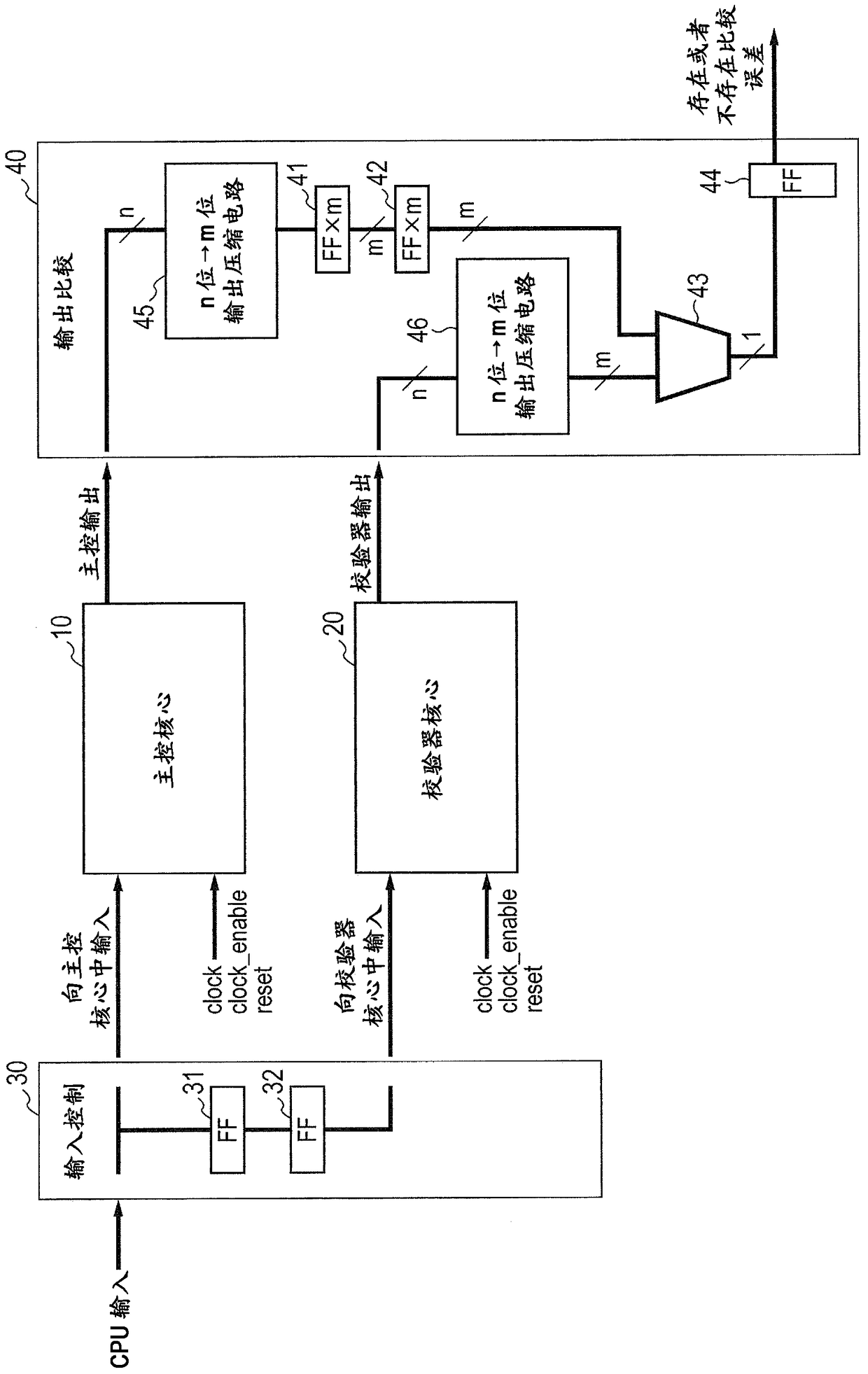
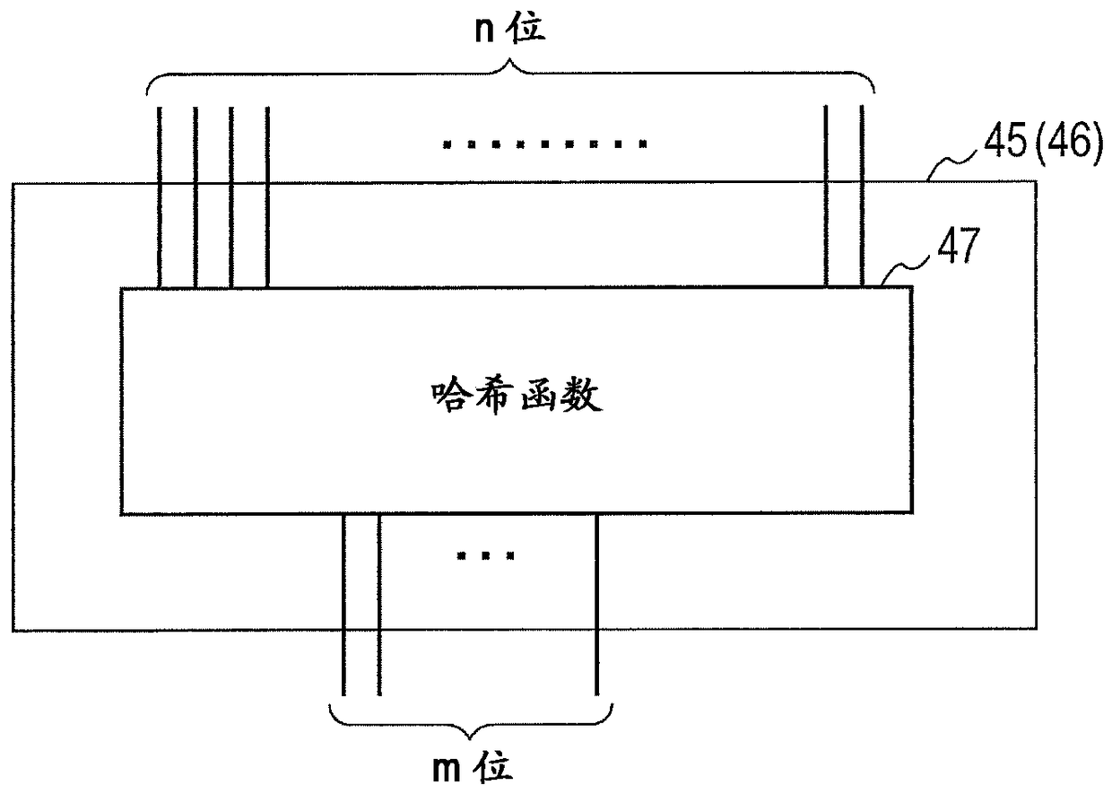
[0054] Figure 4 is a diagram showing an example of the configuration of the n-bit to m-bit output compression circuit 45 (or 46 ) according to the second embodiment. In the second embodiment, the n-bit to m-bit output compression circuit 45 (or 46 ) is configured in such a manner that a signal of n bits is decomposed into groups and the compression level of each group is set variable. In other words, a signal of n-bit width is decomposed into m groups (first group of p1-bit width, second group of p2-bit width to m-th group of pm-bit width). exist Figure 4 The relationship between p1, p2 to pm, m and n in is given by equation (1).

[0055]

[0056] p1 input XOR (exclusive OR) gate 47 1 to pm input XOR gate 47 m is a hash function that maps a p1-bit-wide signal to a pm-bit-wide signal to a 1-bit-wide hash value (1 or 0), respectively. For example input XOR gate 47 to p1 1 Enter the first set of p1 bit widths in . p1 input XOR gate 47 1 Outputs the XOR logical sum (1...

no. 3 example

[0064] Figure 5 is a diagram showing an example of the configuration of the n-bit to m-bit output compression circuit 45 (or 46 ) according to the third embodiment. It will be assumed here that the figure 2 The entire configuration of the semiconductor device according to the third embodiment is shown in . The n-bit to m-bit output compression circuit 45 (or 46) will be described below.

[0065] refer to Figure 5 , in the n-bit to m-bit output compression circuit 45 (or 46) according to the third embodiment, an n-bit-wide signal is decomposed into some signal groups, and the compression level for the groups is set to be variable. However, important signals (of d-bit width) such as address signals, data signals or control signals (for example bus requests or bus responses) are not compressed, for example. Decompose other signals into s groups (where s is the number of groups), that is, p1-bit-wide groups, p2-bit-wide groups to ps-bit-wide groups (group 1 to group s), and...


PUM


Abstract

A semiconductor device comprising: a first processor; a second processor; a first delay circuit delaying a signal input into the first processor by a predefined number of cycles and inputting the signal into the second processor; a first compression circuit compressing a signal of n-bit width from the first processor into a signal of m-bit width (m<n) and outputting the signal of m-bit width; a second compression circuit compressing a signal of n-bit width from the second processor into a signal of m-bit width and outputting the signal of m-bit width; a second delay circuit delaying the signal from the first compressor by the predefined number of cycles and outputting the delayed signal; and a coincidence comparison circuit comparing bit-wise the corresponding bits of the signals from the second delay circuit and from the second compression circuit to check whether the corresponding bits coincide with each other or not.

Description

[0001] Cross References to Related Applications [0002] The disclosure of Japanese Patent Application No. 2012-230383 filed on Oct. 18, 2012 including the specification, drawings and abstract of the specification is hereby incorporated by reference in its entirety. technical field [0003] The present invention relates to a semiconductor device, and more particularly, to a semiconductor device including a processor (CPU core). Background technique [0004] It is required to quickly and accurately detect errors (failures) of semiconductor devices while the semiconductor devices are operating in order to improve the functional safety of the semiconductor devices and the like. Here, functional safety means the safety achieved by the correct operation of safety functions. For example, there is ISO26262 stipulated by ISO (International Organization for Standardization) as a functional safety standard for in-vehicle electronic devices and the like. As a means for embodying a f...

Claims


Application Information

Patent Timeline
Patent Type & Authority Patents(China)
IPC IPC(8): G06F11/00
CPCG06F11/10G06F11/1641G06F11/1695G06F2201/83
Inventor 伊藤雅之
Owner RENESAS ELECTRONICS CORP
Why Eureka
Try Eureka