

Circuit applied to multiple scan modes for testing
a technology of circuits and scan modes, applied in the field of circuits, can solve problems such as the inability to control or measure circuit blocks belonging to other scan modes, and achieve the effect of increasing the circuit area
- Summary
- Abstract
- Description
- Claims
- Application Information
AI Technical Summary
Benefits of technology
Problems solved by technology
Method used
Image

Examples
Embodiment Construction
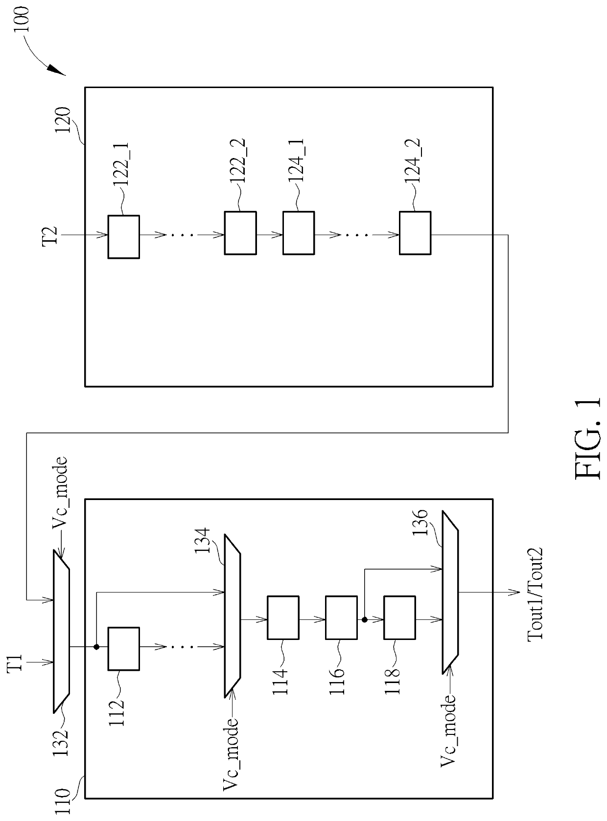
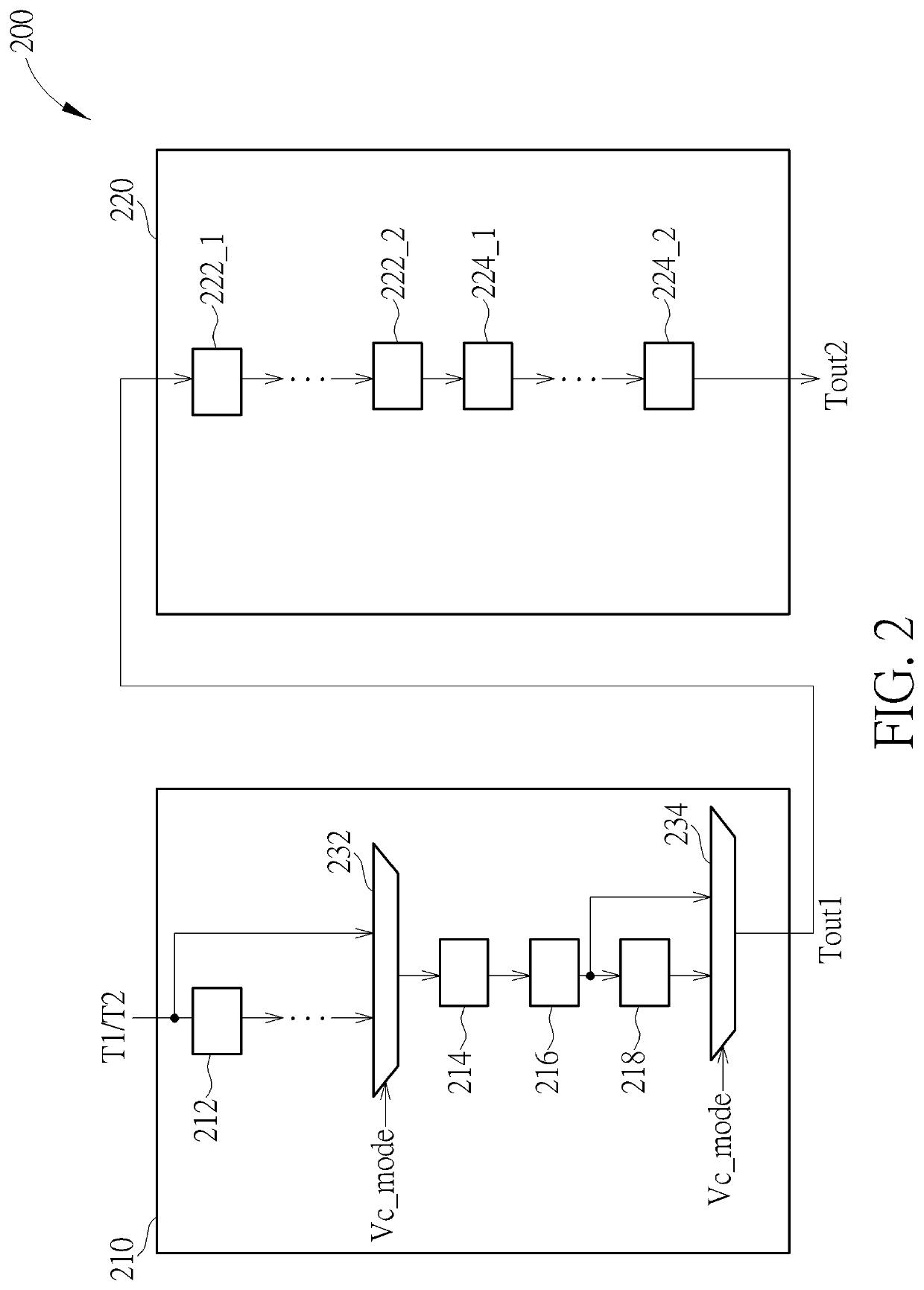
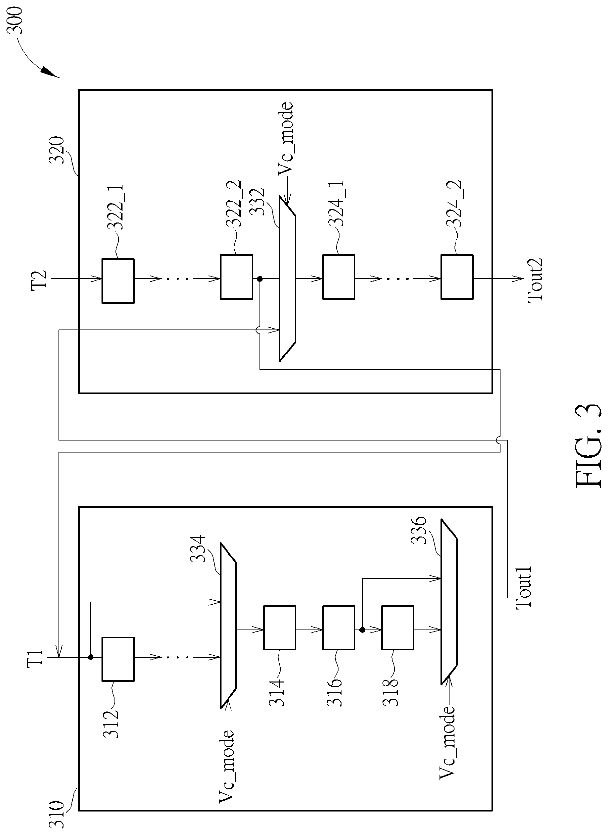
[0015]FIG. 1 is a diagram illustrating a chip 100 applied to multiple scan modes for testing according to an embodiment of the present invention. As shown in FIG. 1, the chip 100 comprises a first circuit block 110 and a second circuit block 120, where the first circuit block 110 and the second circuit block 120 respectively correspond to a first scan mode and a second scan mode, and the first scan mode and the second scan mode respectively receive a first test signal T1 and a second test signal T2 from an external automatic test equipment (not shown) at different time points, to test whether functions of the first circuit block 110 and the second circuit block 120 are correct. Both the first circuit block 110 and the second circuit block 120 comprise a plurality of scan chains to connect a plurality of logic circuits in series for testing, but only two scan chains are illustrated in FIG. 1.
[0016]In this embodiment, the first circuit block 110 comprises several flip-flops 112, 114, ...
PUM
 Abstract
Description
Claims
Application Information