jfet and its manufacturing method
A manufacturing method and technology of conductivity type, applied in the field of JFET manufacturing and junction field effect transistor, can solve the problems of low doping concentration, great variation of substrate resistivity, unstable performance of JFET, etc.
- Summary
- Abstract
- Description
- Claims
- Application Information
AI Technical Summary
Problems solved by technology
Method used
Image


Examples
Embodiment Construction
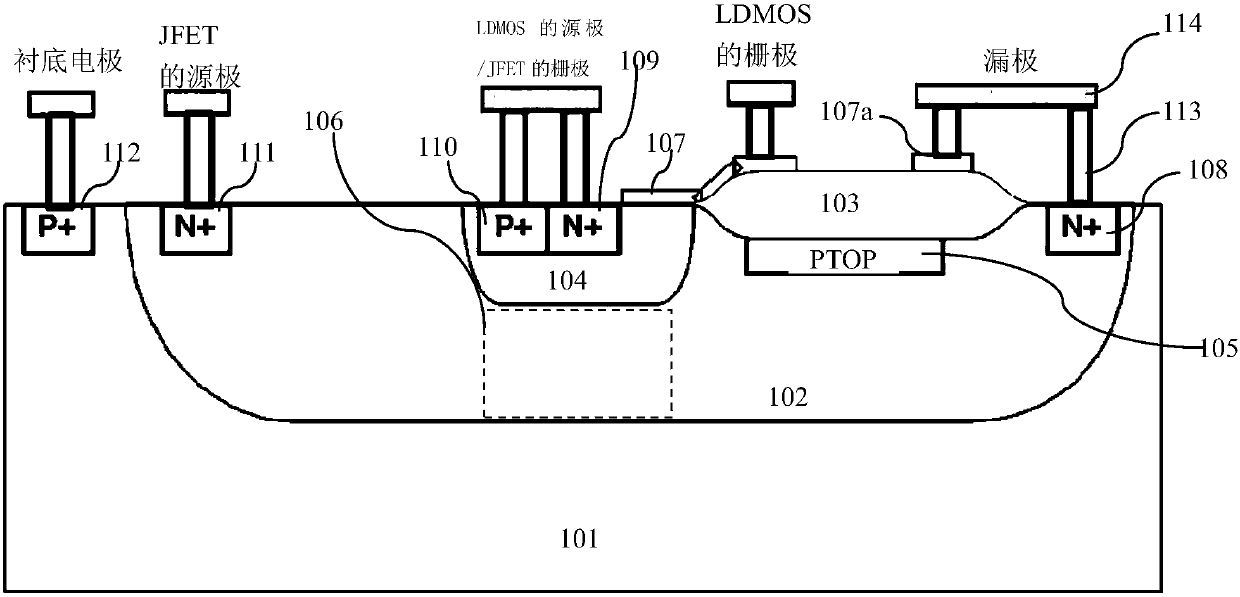
[0065] like figure 1 Shown is a schematic structural diagram of an existing JFET; JFET is integrated in LDMOS, taking an N-type device as an example, an N-type deep well 102 is formed in a P-type semiconductor substrate such as a P-type silicon substrate 101, and an N-type deep well 102 is formed in a P-type semiconductor substrate such as a P-type silicon substrate 101. A field oxide layer 103 is formed on the surface of the P-type silicon substrate 101 of the P-type deep well 102 . The P-type well region 104 is formed in the N-type deep well 102, and the P-type well region 104 is simultaneously used as the channel region of the LDMOS and the gate region of the JFET; a PTOP is formed on the surface of the N-type deep well 102 at the bottom of the field oxide layer 103 Layer 105. The N+ doped drain region 108 shared by JFET and LDMOS is formed on the surface of N-type deep well 102, and the drift region shared by JFET and LDMOS is composed of N-type deep well 102 between drai...
PUM
 Abstract
Description
Claims
Application Information
 - R&D
- Intellectual Property
- Life Sciences
- Materials
- Tech Scout
- Unparalleled Data Quality
- Higher Quality Content
- 60% Fewer Hallucinations
Browse by: Latest US Patents, China's latest patents, Technical Efficacy Thesaurus, Application Domain, Technology Topic, Popular Technical Reports.
© 2025 PatSnap. All rights reserved.Legal|Privacy policy|Modern Slavery Act Transparency Statement|Sitemap|About US| Contact US: help@patsnap.com