A 3D Metamaterial Decoupling Structure for Microstrip Array Antenna

A technology of microstrip array and metamaterials, which is applied in the direction of antenna grounding switch structure connection, antenna coupling, and radiation element structure, can solve the problem of isolation reduction, achieve improved isolation, reduce side lobe level, and balance feed The effect of electricity

CN106848583BActive Publication Date: 2019-09-27HARBIN ENG UNIV
3 Cites 0 Cited by

Patent Information

Authority / Receiving Office
CN · China
Patent Type
Patents(China)
Current Assignee / Owner
Publication Date
2019-09-27

Smart Images

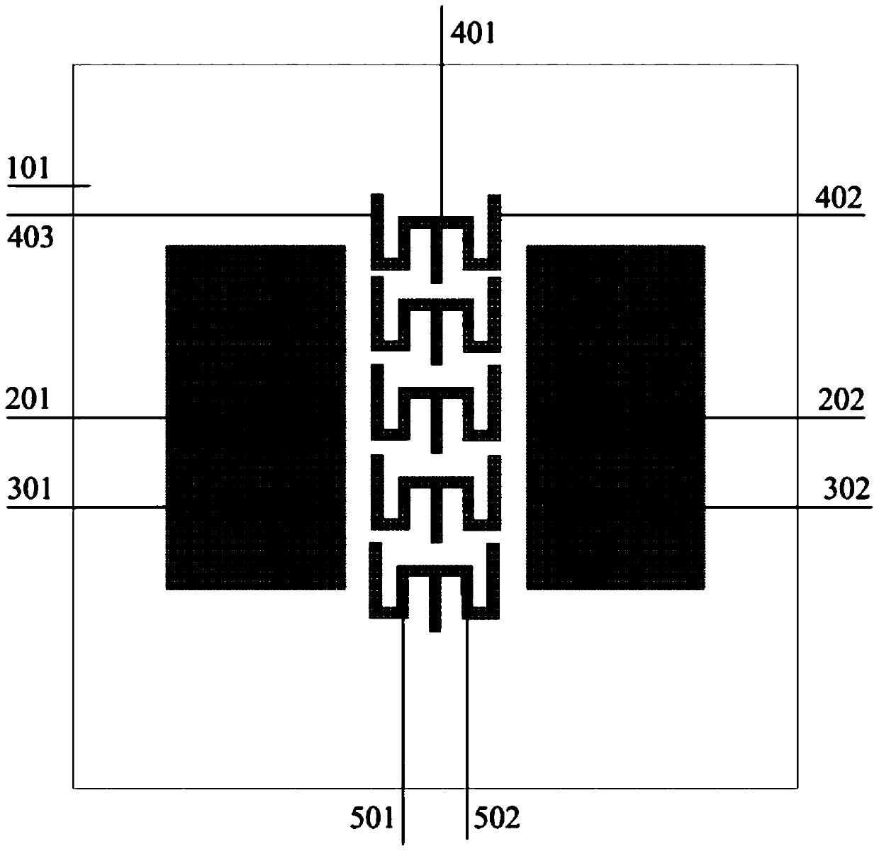
  • Figure 1
    Figure 1
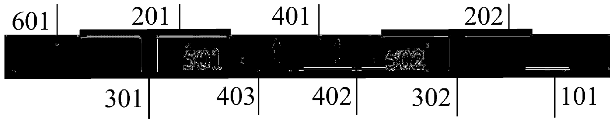
  • Figure 2
    Figure 2
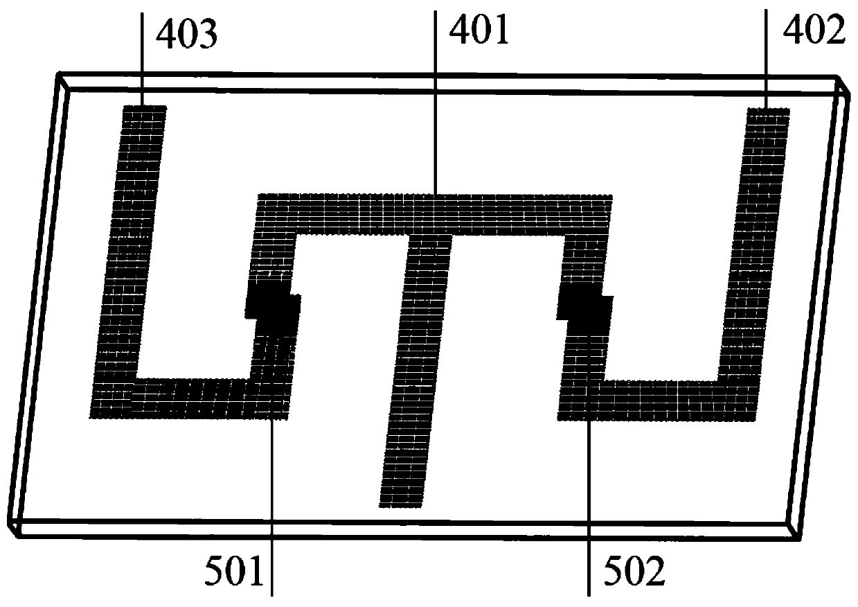
  • Figure 3
    Figure 3
Patent Text Reader

Abstract

The invention provides a three-dimensional metamaterial decoupling structure used for a microstrip array antenna. The structure comprises a public grounding plate, a dielectric substrate on the public grounding plate, two rectangular radiation patches symmetrically arranged on the upper surface of the dielectric substrate, and two coaxial feed ports, wherein five three-dimensional metamaterial decoupling units are embedded in the portion, between the two rectangular radiation patches, in the dielectric substrate in a row. By embedding the five three-dimensional metamaterial decoupling units in a dielectric between microstrip antenna array elements, intercoupling between the microstrip antenna array elements is effectively reduced, and accordingly the isolation of an antenna array is improved.
Need to check novelty before this filing date? Find Prior Art

Description

technical field

[0001] The invention relates to a three-dimensional metamaterial decoupling structure for a microstrip array antenna. Background technique

[0002] Since the array antenna has high gain and strong directivity, it can improve transmission capacity and transmission quality. In recent years, antenna arrays have been widely used in the field of radio communication. At the same time, with the development of wireless communication technology, users' requirements for the integration of communication equipment are increasing year by year, and the research on the miniaturization of array antennas has also received more and more attention. The isolation between the elements of the antenna array will affect the performance of the wireless communication system, such as the radiation efficiency of the antenna or the error of amplitude and phase. Therefore, research on antenna arrays has always been restricted by bottlenecks such as mutual coupling between array elements...

Examples

Embodiment Construction

[0017] The present invention will be further described in detail below in conjunction with the accompanying drawings and specific embodiments.

[0018] Such as figure 1 and figure 2 As shown, the present invention includes a common ground plane 101 printed on the lower surface of the dielectric substrate, rectangular radiation patches 201 and 202 printed on the upper surface of the dielectric substrate, two coaxial feed ports 301 and 302, and a metamaterial structural unit top sticker Sheet 401 , bottom patches 402 and 403 of the metamaterial structural unit, two short-circuit probes 501 and 502 connecting the top and bottom of the metamaterial structural unit.

[0019] The dielectric substrate 601 is an FR4 dielectric with a dielectric constant of 4.4. In order to reduce design costs, the length and width of the dielectric substrate 601 are designed according to the miniaturization design of the antenna array and the radiation pattern requirements, that is, the dielectric s...