Array substrate, display panel and display device

A technology of array substrate and substrate substrate, applied in optics, instruments, electrical digital data processing, etc., can solve the problem of high process requirements

Active Publication Date: 2017-06-16
XIAMEN TIANMA MICRO ELECTRONICS
View PDF7 Cites 3 Cited by
  • Summary
  • Abstract
  • Description
  • Claims
  • Application Information

AI Technical Summary

Problems solved by technology

[0005] In view of this, an embodiment of the present invention provides an array substrate, a display panel and a display device to solve the technical problem of high process requirements in the preparation process of existing TED display devices

Method used


Image

  • Array substrate, display panel and display device
  • Array substrate, display panel and display device
  • Array substrate, display panel and display device

Examples


Embodiment Construction

[0023] In order to make the purpose, technical solution and advantages of the present invention clearer, the technical solution of the present invention will be fully described below through specific implementation in combination with the drawings in the embodiments of the present invention. Apparently, the described embodiments are some embodiments of the present invention, rather than all embodiments. Based on the embodiments of the present invention, all other embodiments obtained by persons of ordinary skill in the art without making creative efforts, All fall within the protection scope of the present invention.

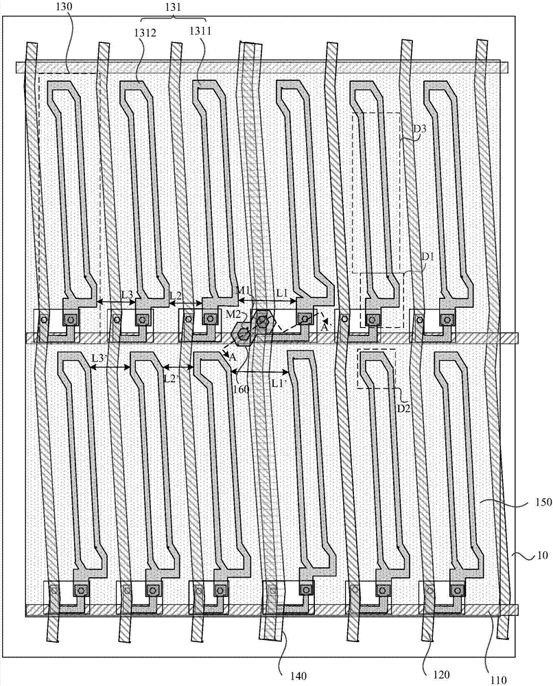
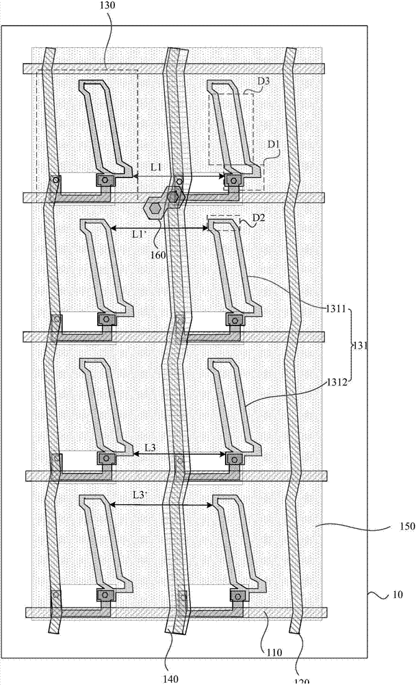
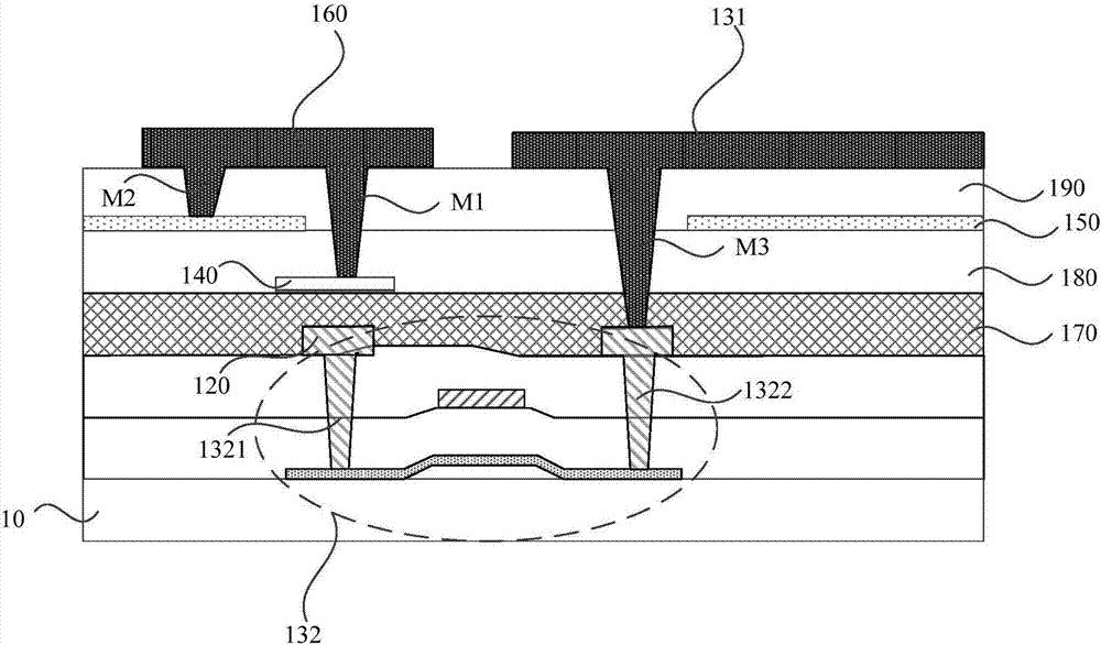
[0024] figure 1 is a schematic top view structure diagram of an array substrate provided by an embodiment of the present invention, please refer to figure 1 , the array substrate includes:

[0025] base substrate 10;

[0026] A plurality of scanning lines 110 and a plurality of data lines 120 formed on the base substrate 10, the plurality of scanning lines 11...


PUM


Abstract

The embodiment of the invention discloses an array substrate, a display panel and a display device. The array substrate comprises a substrate base plate, multiple scan lines and multiple data lines, wherein the multiple scan lines and the multiple data lines define multiple pixel units in an insulated and crossed mode, and pixel electrodes electrically connected with the data lines are arranged in the pixel units. A touch wire is electrically connected with one corresponding touch electrode through a bridge-across structure. The bridge-across structure is arranged at the crossed position of at least one pixel electrode and is arranged at the same layer with the pixel electrodes. Each pixel electrode comprises two end electrodes in the data line extending direction. In the scan line extending direction, the distances between the end electrodes of two adjacent first-type pixel electrodes are greater than those between the end electrodes of the first-type pixel electrodes and second-type pixel electrodes which are adjacent and are greater than or equal to those between the end electrodes of two adjacent second-type pixel electrodes. In conclusion, the distances between the end electrodes of the pixel electrodes and the bridge-across structures are larger, the process requirement is simple, and the production cost is low.

Description

technical field [0001] Embodiments of the present invention relate to the technical field of semiconductors, and in particular, to an array substrate, a display panel, and a display device. Background technique [0002] Liquid Crystal Display (LCD) is a kind of flat panel display. With the development of science and technology, LCD's current technology information products are also developing towards the goal of being light, thin, short, and small. Whether it is a right-angle display, low power consumption, small size, or zero radiation, it can be enjoyed by users. Optimal visual environment. [0003] A display with a touch function is produced based on a function-enriching technology. Common touch technologies include In-cell touch technology and On-cell touch technology. Among them, In-cell touch technology refers to the technology of integrating the touch structure into the array substrate or the opposite substrate of the display panel, and On-cell touch technology refe...

Claims


Application Information

Patent Timeline
Patent Type & Authority Applications(China)
IPC IPC(8): G02F1/1362G02F1/1333G06F3/041
CPCG02F1/13338G02F1/136286G06F3/0412
Inventor 杨倩彭涛周秀峰
Owner XIAMEN TIANMA MICRO ELECTRONICS
Why Eureka
Try Eureka