Substrate, semiconductor device and substrate manufacturing method

A manufacturing method and substrate technology, applied in the direction of semiconductor devices, electrical components, circuits, etc., can solve problems such as difficult etching and patterning, achieve convenient testing methods, ensure etching accuracy, and improve crystal growth quality Effect

Active Publication Date: 2020-02-04
SUZHOU INST OF NANO TECH & NANO BIONICS CHINESE ACEDEMY OF SCI
View PDF7 Cites 0 Cited by
  • Summary
  • Abstract
  • Description
  • Claims
  • Application Information

AI Technical Summary

Problems solved by technology

[0004] However, due to the stable chemical and physical properties of sapphire, it is difficult to etch and pattern

Method used


Image

  • Substrate, semiconductor device and substrate manufacturing method
  • Substrate, semiconductor device and substrate manufacturing method

Examples


Embodiment Construction

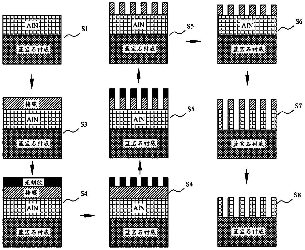
[0035] The embodiment of the present application discloses a substrate, including a sapphire substrate and a patterned AlN thin film formed on the sapphire substrate.

[0036] Preferably, the thickness of the AlN thin film is 3-15 μm.

[0037] The application also discloses a semiconductor device, including the substrate and an epitaxial layer formed on the substrate.

[0038] In this technical solution, the semiconductor device is preferably a III-V LED device. In some embodiments, the semiconductor device may also be other AlN-based devices such as surface acoustic wave devices, high-frequency high-power devices, and the like.

[0039] The present application also discloses a method for manufacturing a substrate. First, the mask material is evaporated, and then the mask is etched by dry method, and AlN is etched by wet method, and finally the mask material is removed, thereby forming a patterned AlN film. method, using this method, a patterned AlN film on an AlN / sapphire t...


PUM

PropertyMeasurementUnit
thicknessaaaaaaaaaa
thicknessaaaaaaaaaa
thicknessaaaaaaaaaa

Abstract

The application discloses a substrate, a semiconductor device and a manufacturing method of the substrate. The substrate includes a sapphire substrate and a patterned AlN thin film formed on the sapphire substrate. The semiconductor device includes the substrate and an epitaxial layer formed on the substrate. The manufacturing method of the substrate includes: first evaporating mask material, then performing dry etching mask, then etching AlN by wet method, and finally removing mask material to form a patterned AlN thin film. In the present invention, a patterned AlN thin film can be prepared on an AlN / sapphire template by using a conventional process. The combination of dry etching and wet etching is used to ensure both etching accuracy and etching rate. The requirement for the preparation process is very simple, and the testing method is convenient. The invention uses AlN / sapphire template to etch AlN to prepare periodic patterns on the AlN thin film, so as to achieve the purpose of improving crystal growth quality and improving device efficiency.

Description

technical field [0001] The present application belongs to the technical field of semiconductors, and in particular relates to a substrate, a semiconductor device and a substrate manufacturing method. Background technique [0002] AlN is one of the semiconductors with the widest band gap among III-V semiconductor materials. The band gap at room temperature is about 6.2eV. It is a direct band gap semiconductor material, and the emission wavelength of the inter-band transition corresponds to the deep ultraviolet band; AlN has good Chemical stability, high thermal conductivity, thermal stability, good dielectric properties, and good physical properties, such as high breakdown field strength, high thermal conductivity, fast electron saturation drift, etc., in deep ultraviolet LED, ultraviolet LD, surface acoustic wave devices and high-frequency high-power devices have good application prospects. Although the research on AlN-based devices has made some progress in recent years, t...

Claims


Application Information

Patent Timeline
Patent Type & Authority Patents(China)
IPC IPC(8): H01L33/00H01L33/22
CPCH01L33/0066H01L33/0075H01L33/22
Inventor 李雪威张纪才王建峰徐科
Owner SUZHOU INST OF NANO TECH & NANO BIONICS CHINESE ACEDEMY OF SCI
Why Eureka
Try Eureka